System Reference Manual
THIS DOCUMENT

This work is licensed under a Creative Commons Attribution-ShareAlike 4.0 International License
All derivative works are to be attributed to Jason Kridner of BeagleBoard.org.
Supply comments and errors via https://github.com/beagleboard/beaglebone-ai/issues.
All information in this document is subject to change without notice.
For an up to date version of this document refer to:
- 1 Introduction
- 2 Change History
- 3 Connecting Up Your BeagleBone AI
- 4 BeagleBone AI Overview
- 5 BeagleBone AI High Level Specification
- 6 Detailed Hardware Design
-
7 Connectors
-
7.1 Expansion Connectors
-
7.1.1 Connector P8
- 7.1.1.1 P8.01-P8.02
- 7.1.1.2 P8.03-P8.05
- 7.1.1.3 P8.06-P8.09
- 7.1.1.4 P8.10-P8.13
- 7.1.1.5 P8.14-P8.16
- 7.1.1.6 P8.17-P8.19
- 7.1.1.7 P8.20-P8.22
- 7.1.1.8 P8.23-P8.26
- 7.1.1.9 P8.27-P8.29
- 7.1.1.10 P8.30-P8.32
- 7.1.1.11 P8.33-P8.35
- 7.1.1.12 P8.36-P8.38
- 7.1.1.13 P8.39-P8.41
- 7.1.1.14 P8.42-P8.44
- 7.1.1.15 P8.45-P8.46
- 7.1.2 Connector P9
-
7.1.1 Connector P8
- 7.2 Serial Debug
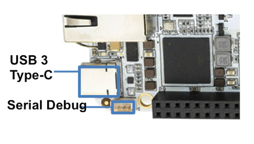
- 7.3 USB 3 Type-C
- 7.4 USB 2 Type-A
- 7.5 Gigabit Ethernet
- 7.6 Coaxial
- 7.7 microSD Memory
- 7.8 microHDMI
-
7.1 Expansion Connectors
-
8 Cape Board Support
- 8.1 BeagleBone® Black Cape Compatibility
- 8.2 EEPROM
- 8.3 Pin Usage Consideration
- 8.4 GPIO
- 8.5 I2C
- 8.6 UART or PRU UART
- 8.7 SPI
- 8.8 Analog
- 8.9 PWM, TIMER, eCAP or PRU PWM/eCAP
- 8.10 eQEP
- 8.11 CAN
- 8.12 McASP (audio serial like I2S and AC97)
- 8.13 MMC
- 8.14 LCD
- 8.15 PRU GPIO
- 8.16 CLKOUT
- 8.17 Expansion Connector Headers
- 8.18 Signal Usage
- 8.19 Cape Power
- 8.20 Mechanical
- 9 Mechanical Information
- 10 Pictures
- 11 Support Information
- 12 Terms and Conditions
TODO: Add image
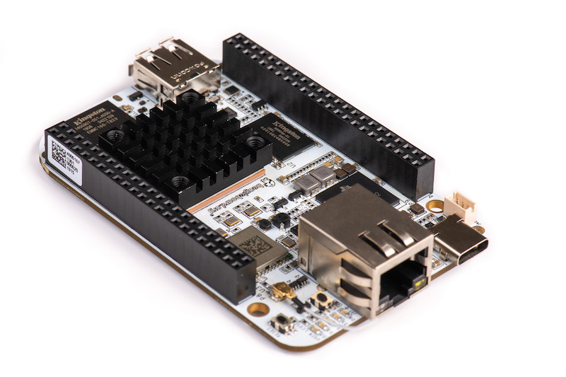
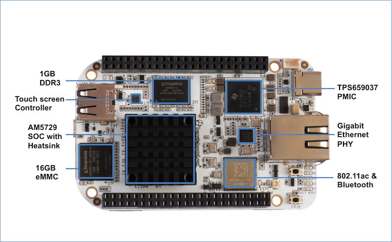
Built on the proven BeagleBoard.org® open source Linux approach, BeagleBone® AI fills the gap between small SBCs and more powerful industrial computers. Based on the Texas Instruments AM5729, developers have access to the powerful SoC with the ease of BeagleBone® Black header and mechanical compatibility. BeagleBone® AI makes it easy to explore how artificial intelligence (AI) can be used in everyday life via TI C66x digital-signal-processor (DSP) cores and embedded-vision-engine (EVE) cores supported through an optimized TIDL machine learning OpenCL API with pre-installed tools. Focused on everyday automation in industrial, commercial and home applications.
Initial prototype revision. Not taken to production.
eMMC flash image provided by Embest.
Second round prototype.
-
Fixed size of mounting holes.
-
Added LED for WiFi status.
-
Added microHDMI.
-
Changed eMMC voltage from 3.3V to 1.8V to support HS200.
-
Changed eMMC from 4GB to 16GB.
-
Changed serial debug header from 6-pin 100mil pitch to 3-pin 1.5mm pitch.
-
Switched expansion header from UART4 to UART5. The UART4 pins were used for the microHDMI.
eMMC flash image provided by Embest.
Alpha pilot-run units and initial production.
Alpha pilot-run eMMC flash image: https://debian.beagleboard.org/images/bbai-pilot-20190408.img.xz
Production eMMC flash image: http://debian.beagleboard.org/images/am57xx-eMMC-flasher-debian-9.9-lxqt-armhf-2019-08-03-4gb.img.xz
BeagleBone® AI comes in the box with the heat sink and antenna already
attached. Developers can get up and running in five minutes with no microSD
card needed. BeagleBone® AI comes preloaded with a Linux distribution.
In the box you will find:
-
BeagleBone® AI
-
Quick Start Guide
TODO: Add links to the design materials for both

You will need to purchase:
-
USB C cable or USB C to USB A cable
-
MicroSD Card (optional)
-
Serial cable[https://github.com/beagleboard/beaglebone-ai/wiki/Frequently-Asked-Questions#serial-cable] (optional)
More information or to purchase a replacement heat sink or antenna, please go to these web sites:
The pre-attached heat sink has M3 holes spaced 20x20 mm. The height of the heat sink clears the USB type A socket, and all other components on the board except the 46-way header sockets and the Ethernet socket.
If you run all of the accelerators or have an older software image, you’ll likely need fan. To find a fan, visit the link to fans in the FAQ.
|
🔥
|
BeagleBone AI can run HOT! Even without running the accelerators, getting up to 70C is not uncommon. |
Official BeagleBone Fan Cape: https://www.newark.com/element14/6100310/beaglebone-ai-fan-cape/dp/50AH3704
TODO: create short-links for any long URLs so that text works.
This section will describe how to connect the board for use. The board can be configured in several different ways. Below we will walk through the most common scenarios. NOTE: These connection scenarios are dependent on the software image presently on your BeagleBone® AI. When all else fails, follow the instructions at https://beagleboard.org/upgrade
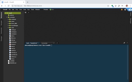
The most common way to program BeagleBone® AI is via a USB connection to a PC. If your computer has a USB C type port, BeagleBone® AI will both communicate and receive power directly from the PC. If your computer does not support USB C type, you can utilize a powered USB C hub to power and connect to BeagleBone® AI which in turn will connect to your PC. You can also use a powered USB C hub to power and connect peripheral devices such as a USB camera. After booting, the board is accessed either as a USB storage device or via the browser on the PC. You will need Chrome or Firefox on the PC.
NOTE:Start with this image "am57xx-eMMC-flasher-debian-10.3-iot-tidl-armhf-2020-04-06-6gb.img.xz" loaded on your BeagleBone® AI.
-
Locate the USB Type-C connector on BeagleBone® AI
-
Connect a USB type-C cable to BeagleBone® AI USB type-C port.

-
Connect the other end of the USB cable to the PC USB 3 port.

-
BeagleBone® AI will boot.
-
You will notice some of the 5 user LEDs flashing
-
Look for a new mass storage drive to appear on the PC.
-
Open the drive and open START.HTM with your web browser.

-
Follow the instructions in the browser window.

-
Go to Cloud9 IDE

-
Open the directories in the left navigation of Cloud9

NOTE:This configuration requires loading the latest debian 9 image from https://elinux.org/Beagleboard:Latest-images-testing
Load "am57xx-eMMC-flasher-debian-9.13-lxqt-tidl-armhf-2020-08-25-6gb.img.xz" image on the BeagleBone® AI
Presently, the "Cloud 9" application is broken in debian 10 only for this configuration. We re working on a better solution.
-
Connect a combo keyboard and mouse to BeagleBone® AI’s USB host port.
-
Connect a microHDMI-to-HDMI cable to BeagleBone® AI’s microHDMI port.
-
Connect the microHDMI-to-HDMI cable to an HDMI monitor.
-
Plug a 5V 3A USB type-C power supply into BeagleBone® AI’s USB type-C port.
-
BeagleBone® AI will boot. No need to enter any passwords.
-
Depending on which software image is loaded, either a Desktop or a login shell will appear on the monitor.
-
Follow the instructions at https://beagleboard.org/upgrade
NOTE:Start with this image "am57xx-eMMC-flasher-debian-10.3-iot-tidl-armhf-2020-04-06-6gb.img.xz" loaded on your BeagleBone® AI.
-
Plug a 5V 3A USB type-C power supply into BeagleBone® AI’s USB type-C port.
-
BeagleBone® AI will boot.
-
Connect your PC’s WiFi to SSID "BeagleBone-XXXX" where XXXX varies for your BeagleBone® AI.
-
Use password "BeagleBone" to complete the WiFi connection.
-
Open http://192.168.8.1 in your web browser.
-
Follow the instructions in the browser window.
A 3 PIN serial debug cable can be helpful to debug when you need to view the boot messages through a terminal program such as putty on your host PC. This cable is not needed for most BeagleBone® AI boot up scenarios.
Cables: https://github.com/beagleboard/beaglebone-ai/wiki/Frequently-Asked-Questions#serial-cable
Locate the 3 PIN debug header on BeagleBone® AI, near the USB C connection.
Press the small white connector into the 3 PIN debug header. The pinout is:
Pin 1 (the pin closest to the screw-hole in the board. It is also marked with a shape on the silkscreen): GND
Pin 2: UART1_RX (i.e. this is a BB-AI input pin)
Pin 3: UART1_TX (i.e. BB-AI transmits out on this pin)

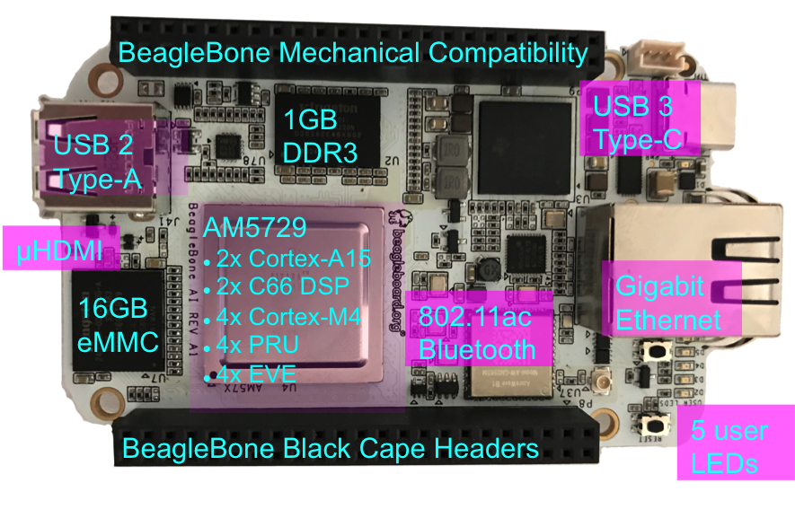
Main Processor Features of the AM5729 Within BeagleBone® AI
-
Dual 1.5GHz ARM® Cortex®-A15 with out-of-order speculative issue 3-way superscalar execution pipeline for the fastest execution of existing 32-bit code
-
2 C66x Floating-Point VLIW DSP supported by OpenCL
-
4 Embedded Vision Engines (EVEs) supported by TIDL machine learning library
-
2x Dual-Core Programmable Real-Time Unit (PRU) subsystems (4 PRUs total) for ultra low-latency control and software generated peripherals
-
2x Dual ARM® Cortex®-M4 co-processors for real-time control
-
IVA-HD subsystem with support for 4K @ 15fps H.264 encode/decode and other codecs @ 1080p60
-
Vivante® GC320 2D graphics accelerator
-
Dual-Core PowerVR® SGX544™ 3D GPU
Communications
-
BeagleBone Black header and mechanical compatibility
-
16-bit LCD interfaces
-
4+ UARTs
-
2 I2C ports
-
2 SPI ports
-
Lots of PRU I/O pins
Memory
-
1GB DDR3L
-
16GB on-board eMMC flash
Connectors
-
USB Type-C connector for power and SuperSpeed dual-role controller
-
Gigabit Ethernet
-
802.11ac 2.4/5GHz WiFi via the AzureWave AW-CM256SM
Out of Box Software
-
Zero-download out of box software environment
This section provides the high level specification of BeagleBone® AI
The figure below is the high level block diagram of BeagleBone® AI. For detailed layout information please check the schematics.

The Texas Instruments AM572x Sitara™ processor family of SOC devices brings high processing performance through the maximum flexibility of a fully integrated mixed processor solution. The devices also combine programmable video processing with a highly integrated peripheral set ideal for AI applications. The AM5729 used on BeagleBone® AI is the super-set device of the family.
Programmability is provided by dual-core ARM® Cortex®-A15 RISC CPUs with Arm® Neon™ extension, and two TI C66x VLIW floating-point DSP core, and Vision AccelerationPac (with 4x EVEs). The Arm allows developers to keep control functions separate from other algorithms programmed on the DSPs and coprocessors, thus reducing the complexity of the system software.
Texas Instruments AM572x Sitara™ Processor Family Block Diagram*
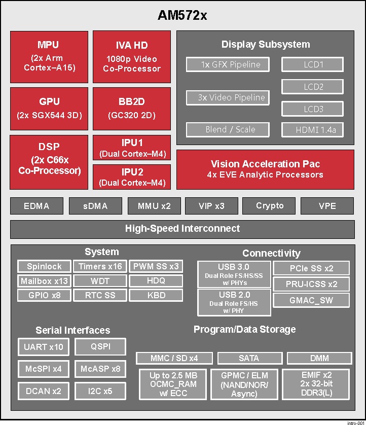
MPU Subsystem The Dual Cortex-A15 MPU subsystem integrates the following submodules:
-
ARM Cortex-A15 MPCore
-
Two central processing units (CPUs)
-
ARM Version 7 ISA: Standard ARM instruction set plus Thumb®-2, Jazelle® RCT Java™ accelerator, hardware virtualization support, and large physical address extensions (LPAE)
-
Neon™ SIMD coprocessor and VFPv4 per CPU
-
Interrupt controller with up to 160 interrupt requests
-
One general-purpose timer and one watchdog timer per CPU – Debug and trace features
-
32-KiB instruction and 32-KiB data level 1 (L1) cache per CPU
-
-
Shared 2-MiB level 2 (L2) cache
-
48-KiB bootable ROM
-
Local power, reset, and clock management (PRCM) module
-
Emulation features
-
Digital phase-locked loop (DPLL)
DSP Subsystems There are two DSP subsystems in the device. Each DSP subsystem contains the following submodules:
-
TMS320C66x™ Floating-Point VLIW DSP core for audio processing, and general-purpose imaging and video processing. It extends the performance of existing C64x+™ and C647x™ DSPs through enhancements and new features.
-
32-KiB L1D and 32-KiB L1P cache or addressable SRAM
-
288-KiB L2 cache
-
-
256-KiB configurable as cache or SRAM
-
32-KiB SRAM
-
Enhanced direct memory access (EDMA) engine for video and audio data transfer
-
Memory management units (MMU) for address management.
-
Interrupt controller (INTC)
-
Emulation capabilities
-
Supported by OpenCL
EVE Subsystems
-
4 Embedded Vision Engines (EVEs) supported by TIDL machine learning library

The Embedded Vision Engine (EVE) module is a programmable imaging and vision processing engine. Software support for the EVE module is available through OpenCL Custom Device model with fixed set of functions. More information is available http://www.ti.com/lit/wp/spry251/spry251.pdf
PRU-ICSS Subsystems
-
2x Dual-Core Programmable Real-Time Unit (PRU) subsystems (4 PRUs total) for ultra low-latency control and software generated peripherals. Access to these powerful subsystems is available through through the P8 and P9 headers. These are detailed in Section 7.
IPU Subsystems There are two Dual Cortex-M4 IPU subsystems in the device available for general purpose usage, particularly real-time control. Each IPU subsystem includes the following components:
-
Two Cortex-M4 CPUs
-
ARMv7E-M and Thumb-2 instruction set architectures
-
Hardware division and single-cycle multiplication acceleration
-
Dedicated INTC with up to 63 physical interrupt events with 16-level priority
-
Two-level memory subsystem hierarchy
-
L1 (32-KiB shared cache memory)
-
L2 ROM + RAM
-
-
64-KiB RAM
-
16-KiB bootable ROM
-
MMU for address translation
-
Integrated power management
-
Emulation feature embedded in the Cortex-M4
IVA-HD Subsystem
-
IVA-HD subsystem with support for 4K @ 15fps H.264 encode/decode and other codecs @ 1080p60 The IVA-HD subsystem is a set of video encoder and decoder hardware accelerators. The list of supported codecs can be found in the software development kit (SDK) documentation.
BB2D Graphics Accelerator Subsystem The Vivante® GC320 2D graphics accelerator is the 2D BitBlt (BB2D) graphics accelerator subsystem on the device with the following features:
-
API support:
-
OpenWF™, DirectFB
-
GDI/DirectDraw
-
-
BB2D architecture:
-
BitBlt and StretchBlt
-
DirectFB hardware acceleration
-
ROP2, ROP3, ROP4 full alpha blending and transparency
-
Clipping rectangle support
-
Alpha blending includes Java 2 Porter-Duff compositing rules
-
90-, 180-, 270-degree rotation on every primitive
-
YUV-to-RGB color space conversion
-
Programmable display format conversion with 14 source and 7 destination formats
-
High-quality, 9-tap, 32-phase filter for image and video scaling at 1080p
-
Monochrome expansion for text rendering
-
32K × 32K coordinate system
-
Dual-Core PowerVR® SGX544™ 3D GPU The 3D graphics processing unit (GPU) subsystem is based on POWERVR® SGX544 subsystem from Imagination Technologies. It supports general embedded applications. The GPU can process different data types simultaneously, such as: pixel data, vertex data, video data, and general-purpose data. The GPU subsystem has the following features:
-
Multicore GPU architecture: two SGX544 cores.
-
Shared system level cache of 128 KiB
-
Tile-based deferred rendering architecture
-
Second-generation universal scalable shader engines (USSE2), multithreaded engines incorporating pixel and vertex shader functionality
-
Present and texture load accelerators
-
Enables to move, rotate, twiddle, and scale texture surfaces.
-
Supports RGB, ARGB, YUV422, and YUV420 surface formats.
-
Supports bilinear upscale.
-
Supports source colorkey.
-
-
Fine-grained task switching, load balancing, and power management
-
Programmable high-quality image antialiasing
-
Bilinear, trilinear, anisotropic texture filtering
-
Advanced geometry DMA driven operation for minimum CPU interaction
-
Fully virtualized memory addressing for OS operation in a unified memory architecture (MMU)
Dual 256M x 16 DDR3L memory devices are used, one on each side of the board, for a total of 1 GB. They will each operate at a clock frequency of up to 533 MHz yielding an effective rate of 1066Mb/s on the DDR3L bus allowing for 4GB/s of DDR3L memory bandwidth.
TODO: Add WiFi/Bluetooth/Ethernet
BeagleBone® AI supports the majority of the functions of the AM5729 SOC through connectors or expansion header pin accessibility. See section 7 for more information on expansion header pinouts. There are a few functions that are not accessible which are: (TBD)
TODO: This text needs to go somewhere.
| Address | Identifier | Description |
|---|---|---|
0x12 |
U3 |
TPS6590379 PMIC DVS |
0x41 |
U78 |
STMPE811Q ADC and GPIO expander |
0x47 |
U13 |
HD3SS3220 USB Type-C DRP port controller |
0x50 |
U9 |
24LC32 board ID EEPROM |
0x58 |
U3 |
TPS6590379 PMIC power registers |
0x5a |
U3 |
TPS6590379 PMIC interfaces and auxilaries |
0x5c |
U3 |
TPS6590379 PMIC trimming and test |
0x5e |
U3 |
TPS6590379 PMIC OTP |
This section provides a detailed description of the Hardware design. This can be useful for interfacing, writing drivers, or using it to help modify specifics of your own design.
The figure below is the high level block diagram of BeagleBone® AI. For those who may be concerned, this is the same figure found in section 5. It is placed here again for convenience so it is closer to the topics to follow.
Figure ? is the high level block diagram of the power section of the board.
(Block Diagram for Power)
The Texas Instruments TPS6590379ZWSR device is an integrated power-management IC (PMIC) specifically designed to work well ARM Cortex A15 Processors, such as the AM5729 used on BeagleBone® AI. The datasheet is located here https://www.ti.com/lit/ds/symlink/tps659037.pdf
The device provides seven configurable step-down converters with up to 6 A of output current for memory, processor core, input-output (I/O), or preregulation of LDOs. One of these configurable step-down converters can be combined with another 3-A regulator to allow up to 9 A of output current. All of the step-down converters can synchronize to an external clock source between 1.7 MHz and 2.7 MHz, or an internal fallback clock at 2.2 MHz.
The TPS659037 device contains seven LDO regulators for external use. These LDO regulators can be supplied from either a system supply or a preregulated supply. The power-up and power-down controller is configurable and supports any power-up and power-down sequences (OTP based). The TPS659037 device includes a 32-kHz RC oscillator to sequence all resources during power up and power down. In cases where a fast start up is needed, a 16-MHz crystal oscillator is also included to quickly generate a stable 32-kHz for the system. All LDOs and SMPS converters can be controlled by the SPI or I2C interface, or by power request signals. In addition, voltage scaling registers allow transitioning the SMPS to different voltages by SPI, I2C, or roof and floor control.
One dedicated pin in each package can be configured as part of the power-up sequence to control external resources. General-purpose input-output (GPIO) functionality is available and two GPIOs can be configured as part of the power-up sequence to control external resources. Power request signals enable power mode control for power optimization. The device includes a general-purpose sigma-delta analog-to-digital converter (GPADC) with three external input channels.

Figure 23 below shows how the USB-C power input is connected to the TPS6590379.
TODO: (Schematic screenshoot)

A board identifier is placed on the eMMC in the second linear boot partition (/dev/mmcblk1boot1). Reserved bytes up to 32k (0x8000) are filled with “FF”.
| Name | Size (bytes) | Contents |
|---|---|---|
Header |
4 |
MSB 0xEE3355AA LSB (stored LSB first) |
Board Name |
8 |
Name for board in ASCII “BBONE-AI” = BeagleBone AI |
Version |
4 |
Hardware version code for board in ASCII “00A1” = rev. A1 |
Serial Number |
14 |
Serial number of the board. This is a 14 character string which is: WWYYEMAInnnnnn where:
|
Example:
debian@beaglebone:/var/lib/cloud9$ sudo hexdump -C /dev/mmcblk1boot1
00000000  aa 55 33 ee 42 42 4f 4e  45 2d 41 49 30 30 41 31  |.U3.BBONE-AI00A1|
00000010  31 39 33 33 45 4d 41 49  30 30 30 38 30 33 ff ff  |1933EMAI000803..|
00000020  ff ff ff ff ff ff ff ff  ff ff ff ff ff ff ff ff  |................|
*
00008000  00 00 00 00 00 00 00 00  00 00 00 00 00 00 00 00  |................|
*
00400000
Datasheet https://storage.googleapis.com/wzukusers/user-26561200/documents/5b7d0fe3c3f29Ct6k0QI/AW-CM256SM_DS_Rev%2015_CYW.pdf Wireless connectivity is provided on BeagleBone® AI via the AzureWave Technologies AW-CM256SM IEEE 802.11a/b/g/n/ac Wi-Fi with Bluetooth 4.2 Combo Stamp Module.
This highly integrated wireless local area network (WLAN) solution combines Bluetooth 4.2 and provides a complete 2.4GHz Bluetooth system which is fully compliant to Bluetooth 4.2 and v2.1 that supports EDR of 2Mbps and 3Mbps for data and audio communications. It enables a high performance, cost effective, low power, compact solution that easily fits onto the SDIO and UART combo stamp module.
Compliant with the IEEE 802.11a/b/g/n/ac standard, AW-CM256SM uses Direct Sequence Spread Spectrum (DSSS), Orthogonal Frequency Division Multiplexing (OFDM), BPSK, QPSK, CCK and QAM baseband modulation technologies. Compare to 802.11n technology, 802.11ac provides a big improvement on speed and range.
The AW-CM256SM module adopts a Cypress solution. The module design is based on the Cypress CYP43455 single chip.
High speed wireless connection up to 433.3Mbps transmit/receive PHY rate using 80MHz bandwidth * 1 antennas to support 1(Transmit) and 1(Receive) technology and Bluetooth * WCS (Wireless Coexistence System) * Low power consumption and high performance * Enhanced wireless security * Fully speed operation with Piconet and Scatternet support * 12mm(L) x 12mm(W) x1.65mm(H) LGA package * Dual - band 2.4 GHz and 5GHz 802.11 a/b/g/n/ac * External Crystal
The HDMI interface is aligned with the HDMI TMDS single stream standard v1.4a (720p @60Hz to 1080p @24Hz) and the HDMI v1.3 (1080p @60Hz): 3 data channels, plus 1 clock channel is supported (differential).
TODO: Verify it isn’t better than this. Doesn’t seem right.
The Texas Instruments AM5729 Sitara™ provides 2 Programmable Real-Time Unit Subsystem and Industrial Communciation Subsystems. (PRU-ICSS1 and PRU-ICSS2).
Within each PRU-ICSS are dual 32-bit Load / Store RISC CPU cores: Programmable Real-Time Units (PRU0 and PRU1), shared data and instruction memories, internal peripheral modules and an interrupt controller. Therefore the SoC is providing a total of 4 PRU 32-bit RISC CPU’s:
-
PRU-ICSS1 PRU0
-
PRU-ICSS1 PRU1
-
PRU-ICSS2 PRU0
-
PRU-ICSS2 PRU1
The programmable nature of the PRUs, along with their access to pins, events and all SoC resources, provides flexibility in implmenting fast real-time responses, specialized data handling operations, peripheral interfaces and in off-loading tasks from the other processor cores of the SoC.
Each of the 2 PRU-ICSS (PRU-ICSS1 and PRU-ICSS2) includes the following main features: * 2 Independent programmable real-time (PRU) cores (PRU0 and PRU1) * 21x Enhanced GPIs (EGPIs) and 21x Enhanced GPOs (EGPOs) with asynchronous capture and serial support per each PRU CPU core * One Ethernet MII_RT module (PRU-ICSS_MII_RT) with two MII ports and configurable connections to PRUs * 1 MDIO Port (PRU-ICSS_MII_MDIO) * One Industrial Ethernet Peripheral (IEP) to manage/generate Industrial Ethernet functions * 1 x 16550-compatible UART with a dedicated 192 MHz clock to support 12Mbps Profibus * 1 Industrial Ethernet timer with 7/9 capture and 8 compare events * 1 Enhanced Capture Module (ECAP) * 1 Interrupt Controller (PRU-ICSS_INTC) * A flexible power management support * Integrated switched central resource with programmable priority * Parity control supported by all memories

Resources
-
Great resources for PRU and BeagleBone® has been compiled here https://beagleboard.org/pru
-
The PRU Cookbook provides examples and getting started information https://github.com/MarkAYoder/PRUCookbook
-
Detailed specification is availble at http://processors.wiki.ti.com/index.php/PRU-ICSS
FAQ
-
Q: Is it possible to configure the Ethernet MII to be accessed via a PRU MII?
-
A: TBD
The table below shows which PRU-ICSS1 signals can be accessed on BeagleBone® AI and on which connector and pins they are accessible from. Some signals are accessible on the same pins. Signal Names reveal which PRU-ICSS Subsystem is being addressed. pr1 is PRU-ICSS1 and pr2 is PRU-ICSS2
| SIGNAL NAME | DESCRIPTION | TYPE | PROC | HEADER_PIN | MODE | HEADER_PIN | MODE |
|---|---|---|---|---|---|---|---|
pr1_pru0_gpo0 |
PRU0 General-Purpose Output |
O |
AH6 |
NA |
|||
pr1_pru0_gpo1 |
PRU0 General-Purpose Output |
O |
AH3 |
NA |
|||
pr1_pru0_gpo2 |
PRU0 General-Purpose Output |
O |
AH5 |
NA |
|||
pr1_pru0_gpo3 |
PRU0 General-Purpose Output |
O |
AG6 |
P8_12 |
MODE13 |
||
pr1_pru0_gpo4 |
PRU0 General-Purpose Output |
O |
AH4 |
P8_11 |
MODE13 |
||
pr1_pru0_gpo5 |
PRU0 General-Purpose Output |
O |
AG4 |
P9_15 |
MODE13 |
||
pr1_pru0_gpo6 |
PRU0 General-Purpose Output |
O |
AG2 |
NA |
|||
pr1_pru0_gpo7 |
PRU0 General-Purpose Output |
O |
AG3 |
NA |
|||
pr1_pru0_gpo8 |
PRU0 General-Purpose Output |
O |
AG5 |
NA |
|||
pr1_pru0_gpo9 |
PRU0 General-Purpose Output |
O |
AF2 |
NA |
|||
pr1_pru0_gpo10 |
PRU0 General-Purpose Output |
O |
AF6 |
NA |
|||
pr1_pru0_gpo11 |
PRU0 General-Purpose Output |
O |
AF3 |
NA |
|||
pr1_pru0_gpo12 |
PRU0 General-Purpose Output |
O |
AF4 |
NA |
|||
pr1_pru0_gpo13 |
PRU0 General-Purpose Output |
O |
AF1 |
NA |
|||
pr1_pru0_gpo14 |
PRU0 General-Purpose Output |
O |
AE3 |
NA |
|||
pr1_pru0_gpo15 |
PRU0 General-Purpose Output |
O |
AE5 |
NA |
|||
pr1_pru0_gpo16 |
PRU0 General-Purpose Output |
O |
AE1 |
NA |
|||
pr1_pru0_gpo17 |
PRU0 General-Purpose Output |
O |
AE2 |
P9_26 |
MODE13 |
||
pr1_pru0_gpo18 |
PRU0 General-Purpose Output |
O |
AE6 |
NA |
|||
pr1_pru0_gpo19 |
PRU0 General-Purpose Output |
O |
AD2 |
NA |
|||
pr1_pru0_gpo20 |
PRU0 General-Purpose Output |
O |
AD3 |
NA |
|||
pr1_pru0_gpi0 |
PRU0 General-Purpose Input |
I |
AH6 |
NA |
|||
pr1_pru0_gpi1 |
PRU0 General-Purpose Input |
I |
AH3 |
NA |
|||
pr1_pru0_gpi2 |
PRU0 General-Purpose Input |
I |
AH5 |
NA |
|||
pr1_pru0_gpi3 |
PRU0 General-Purpose Input |
I |
AG6 |
P8_12 |
MODE12 |
||
pr1_pru0_gpi4 |
PRU0 General-Purpose Input |
I |
AH4 |
P8_11 |
MODE12 |
||
pr1_pru0_gpi5 |
PRU0 General-Purpose Input |
I |
AG4 |
P9_15 |
MODE12 |
||
pr1_pru0_gpi6 |
PRU0 General-Purpose Input |
I |
AG2 |
NA |
|||
pr1_pru0_gpi7 |
PRU0 General-Purpose Input |
I |
AG3 |
NA |
|||
pr1_pru0_gpi8 |
PRU0 General-Purpose Input |
I |
AG5 |
NA |
|||
pr1_pru0_gpi9 |
PRU0 General-Purpose Input |
I |
AF2 |
NA |
|||
pr1_pru0_gpi10 |
PRU0 General-Purpose Input |
I |
AF6 |
NA |
|||
pr1_pru0_gpi11 |
PRU0 General-Purpose Input |
I |
AF3 |
NA |
|||
pr1_pru0_gpi12 |
PRU0 General-Purpose Input |
I |
AF4 |
NA |
|||
pr1_pru0_gpi13 |
PRU0 General-Purpose Input |
I |
AF1 |
NA |
|||
pr1_pru0_gpi14 |
PRU0 General-Purpose Input |
I |
AE3 |
NA |
|||
pr1_pru0_gpi15 |
PRU0 General-Purpose Input |
I |
AE5 |
NA |
|||
pr1_pru0_gpi16 |
PRU0 General-Purpose Input |
I |
AE1 |
NA |
|||
pr1_pru0_gpi17 |
PRU0 General-Purpose Input |
I |
AE2 |
P9_26 |
MODE12 |
||
pr1_pru0_gpi18 |
PRU0 General-Purpose Input |
I |
AE6 |
NA |
|||
pr1_pru0_gpi19 |
PRU0 General-Purpose Input |
I |
AD2 |
NA |
|||
pr1_pru0_gpi20 |
PRU0 General-Purpose Input |
I |
AD3 |
NA |
|||
pr1_pru1_gpo0 |
PRU1 General-Purpose Output |
O |
E2 |
NA |
|||
pr1_pru1_gpo1 |
PRU1 General-Purpose Output |
O |
D2 |
P9_20 |
MODE13 |
||
pr1_pru1_gpo2 |
PRU1 General-Purpose Output |
O |
F4 |
P9_19 |
MODE13 |
||
pr1_pru1_gpo3 |
PRU1 General-Purpose Output |
O |
C1 |
P9_41 |
MODE13 |
||
pr1_pru1_gpo4 |
PRU1 General-Purpose Output |
O |
E4 |
NA |
|||
pr1_pru1_gpo5 |
PRU1 General-Purpose Output |
O |
F5 |
P8_18 |
MODE13 |
||
pr1_pru1_gpo6 |
PRU1 General-Purpose Output |
O |
E6 |
P8_19 |
MODE13 |
||
pr1_pru1_gpo7 |
PRU1 General-Purpose Output |
O |
D3 |
P8_13 |
MODE13 |
||
pr1_pru1_gpo8 |
PRU1 General-Purpose Output |
O |
F6 |
NA |
|||
pr1_pru1_gpo9 |
PRU1 General-Purpose Output |
O |
D5 |
P8_14 |
MODE13 |
||
pr1_pru1_gpo10 |
PRU1 General-Purpose Output |
O |
C2 |
P9_42 |
MODE13 |
||
pr1_pru1_gpo11 |
PRU1 General-Purpose Output |
O |
C3 |
P9_27 |
MODE13 |
||
pr1_pru1_gpo12 |
PRU1 General-Purpose Output |
O |
C4 |
NA |
|||
pr1_pru1_gpo13 |
PRU1 General-Purpose Output |
O |
B2 |
NA |
|||
pr1_pru1_gpo14 |
PRU1 General-Purpose Output |
O |
D6 |
P9_14 |
MODE13 |
||
pr1_pru1_gpo15 |
PRU1 General-Purpose Output |
O |
C5 |
P9_16 |
MODE13 |
||
pr1_pru1_gpo16 |
PRU1 General-Purpose Output |
O |
A3 |
P8_15 |
MODE13 |
||
pr1_pru1_gpo17 |
PRU1 General-Purpose Output |
O |
B3 |
P8_26 |
MODE13 |
||
pr1_pru1_gpo18 |
PRU1 General-Purpose Output |
O |
B4 |
P8_16 |
MODE13 |
||
pr1_pru1_gpo19 |
PRU1 General-Purpose Output |
O |
B5 |
NA |
|||
pr1_pru1_gpo20 |
PRU1 General-Purpose Output |
O |
A4 |
NA |
|||
pr1_pru1_gpi0 |
PRU1 General-Purpose Input |
I |
E2 |
NA |
|||
pr1_pru1_gpi1 |
PRU1 General-Purpose Input |
I |
D2 |
P9_20 |
MODE12 |
||
pr1_pru1_gpi2 |
PRU1 General-Purpose Input |
I |
F4 |
P9_19 |
MODE12 |
||
pr1_pru1_gpi3 |
PRU1 General-Purpose Input |
I |
C1 |
P9_41 |
MODE12 |
||
pr1_pru1_gpi4 |
PRU1 General-Purpose Input |
I |
E4 |
NA |
|||
pr1_pru1_gpi5 |
PRU1 General-Purpose Input |
I |
F5 |
P8_18 |
MODE12 |
||
pr1_pru1_gpi6 |
PRU1 General-Purpose Input |
I |
E6 |
P8_19 |
MODE12 |
||
pr1_pru1_gpi7 |
PRU1 General-Purpose Input |
I |
D3 |
P8_13 |
MODE12 |
||
pr1_pru1_gpi8 |
PRU1 General-Purpose Input |
I |
F6 |
NA |
|||
pr1_pru1_gpi9 |
PRU1 General-Purpose Input |
I |
D5 |
P8_14 |
MODE12 |
||
pr1_pru1_gpi10 |
PRU1 General-Purpose Input |
I |
C2 |
P9_42 |
MODE12 |
||
pr1_pru1_gpi11 |
PRU1 General-Purpose Input |
I |
C3 |
P9_27 |
MODE12 |
||
pr1_pru1_gpi12 |
PRU1 General-Purpose Input |
I |
C4 |
NA |
|||
pr1_pru1_gpi13 |
PRU1 General-Purpose Input |
I |
B2 |
NA |
|||
pr1_pru1_gpi14 |
PRU1 General-Purpose Input |
I |
D6 |
P9_14 |
MODE12 |
||
pr1_pru1_gpi15 |
PRU1 General-Purpose Input |
I |
C5 |
P9_16 |
MODE12 |
||
pr1_pru1_gpi16 |
PRU1 General-Purpose Input |
I |
A3 |
P8_15 |
MODE12 |
||
pr1_pru1_gpi17 |
PRU1 General-Purpose Input |
I |
B3 |
P8_26 |
MODE12 |
||
pr1_pru1_gpi18 |
PRU1 General-Purpose Input |
I |
B4 |
P8_16 |
MODE12 |
||
pr1_pru1_gpi19 |
PRU1 General-Purpose Input |
I |
B5 |
NA |
|||
pr1_pru1_gpi20 |
PRU1 General-Purpose Input |
I |
A4 |
NA |
|||
pr1_mii_mt0_clk |
MII0 Transmit Clock |
I |
U5 |
NA |
|||
pr1_mii0_txen |
MII0 Transmit Enable |
O |
V3 |
NA |
|||
pr1_mii0_txd3 |
MII0 Transmit Data |
O |
V5 |
NA |
|||
pr1_mii0_txd2 |
MII0 Transmit Data |
O |
V4 |
NA |
|||
pr1_mii0_txd1 |
MII0 Transmit Data |
O |
Y2 |
NA |
|||
pr1_mii0_txd0 |
MII0 Transmit Data |
O |
W2 |
NA |
|||
pr1_mii0_rxdv |
MII0 Data Valid |
I |
V2 |
NA |
|||
pr1_mii_mr0_clk |
MII0 Receive Clock |
I |
Y1 |
NA |
|||
pr1_mii0_rxd3 |
MII0 Receive Data |
I |
W9 |
NA |
|||
pr1_mii0_rxd2 |
MII0 Receive Data |
I |
V9 |
NA |
|||
pr1_mii0_crs |
MII0 Carrier Sense |
I |
V7 |
NA |
|||
pr1_mii0_rxer |
MII0 Receive Error |
I |
U7 |
NA |
|||
pr1_mii0_rxd1 |
MII0 Receive Data |
I |
V6 |
NA |
|||
pr1_mii0_rxd0 |
MII0 Receive Data |
I |
U6 |
NA |
|||
pr1_mii0_col |
MII0 Collision Detect |
I |
V1 |
NA |
|||
pr1_mii0_rxlink |
MII0 Receive Link |
I |
U4 |
NA |
|||
pr1_mii_mt1_clk |
MII1 Transmit Clock |
I |
C1 |
P9_41 |
MODE11 |
||
pr1_mii1_txen |
MII1 Transmit Enable |
O |
E4 |
NA |
|||
pr1_mii1_txd3 |
MII1 Transmit Data |
O |
F5 |
P8_18 |
MODE11 |
||
pr1_mii1_txd2 |
MII1 Transmit Data |
O |
E6 |
P8_19 |
MODE11 |
||
pr1_mii1_txd1 |
MII1 Transmit Data |
O |
D5 |
P8_14 |
MODE11 |
||
pr1_mii1_txd0 |
MII1 Transmit Data |
O |
C2 |
P9_42 |
MODE11 |
||
pr1_mii_mr1_clk |
MII1 Receive Clock |
I |
C3 |
P9_27 |
MODE11 |
||
pr1_mii1_rxdv |
MII1 Data Valid |
I |
C4 |
NA |
|||
pr1_mii1_rxd3 |
MII1 Receive Data |
I |
B2 |
NA |
|||
pr1_mii1_rxd2 |
MII1 Receive Data |
I |
D6 |
P9_14 |
MODE11 |
||
pr1_mii1_rxd1 |
MII1 Receive Data |
I |
C5 |
P9_16 |
MODE11 |
||
pr1_mii1_rxd0 |
MII1 Receive Data |
I |
A3 |
P8_15 |
MODE11 |
||
pr1_mii1_rxer |
MII1 Receive Error |
I |
B3 |
P8_26 |
MODE11 |
||
pr1_mii1_rxlink |
MII1 Receive Link |
I |
B4 |
P8_16 |
MODE11 |
||
pr1_mii1_col |
MII1 Collision Detect |
I |
B5 |
NA |
|||
pr1_mii1_crs |
MII1 Carrier Sense |
I |
A4 |
NA |
|||
pr1_mdio_mdclk |
MDIO Clock |
O |
D3 |
P8_13 |
MODE11 |
||
pr1_mdio_data |
MDIO Data |
IO |
F6 |
NA |
|||
pr1_edc_latch0_in |
Latch Input 0 |
I |
AG3/E2 |
NA |
|||
pr1_edc_latch1_in |
Latch Input 1 |
I |
AG5 |
NA |
|||
pr1_edc_sync0_out |
SYNC0 Output |
O |
AF2/D2 |
P9_20 |
MODE11 |
||
pr1_edc_sync1_out |
SYNC1 Output |
O |
AF6 |
NA |
|||
pr1_edio_latch_in |
Latch Input |
I |
AF3 |
NA |
|||
pr1_edio_sof |
Start Of Frame |
O |
AF4/F4 |
P9_19 |
MODE11 |
||
pr1_edio_data_in0 |
Ethernet Digital Input |
I |
AF1/E1 |
NA |
|||
pr1_edio_data_in1 |
Ethernet Digital Input |
I |
AE3/G2 |
NA |
|||
pr1_edio_data_in2 |
Ethernet Digital Input |
I |
AE5/H7 |
NA |
|||
pr1_edio_data_in3 |
Ethernet Digital Input |
I |
AE1/G1 |
NA |
|||
pr1_edio_data_in4 |
Ethernet Digital Input |
I |
AE2/G6 |
P9_26 |
MODE10 |
P8_34 |
MODE12 |
pr1_edio_data_in5 |
Ethernet Digital Input |
I |
AE6/F2 |
P8_36 |
MODE12 |
||
pr1_edio_data_in6 |
Ethernet Digital Input |
I |
AD2/F3 |
NA |
|||
pr1_edio_data_in7 |
Ethernet Digital Input |
I |
AD3/D1 |
P8_15 |
MODE12 |
||
pr1_edio_data_out0 |
Ethernet Digital Output |
O |
AF1/E1 |
NA |
|||
pr1_edio_data_out1 |
Ethernet Digital Output |
O |
AE3/G2 |
NA |
|||
pr1_edio_data_out2 |
Ethernet Digital Output |
O |
AE5/H7 |
NA |
|||
pr1_edio_data_out3 |
Ethernet Digital Output |
O |
AE1/G1 |
NA |
|||
pr1_edio_data_out4 |
Ethernet Digital Output |
O |
AE2/G6 |
P9_26 |
MODE11 |
P8_34 |
MODE13 |
pr1_edio_data_out5 |
Ethernet Digital Output |
O |
AE6/F2 |
P8_36 |
MODE13 |
||
pr1_edio_data_out6 |
Ethernet Digital Output |
O |
AD2/F3 |
NA |
|||
pr1_edio_data_out7 |
Ethernet Digital Output |
O |
AD3/D1 |
P8_15 |
MODE13 |
||
pr1_uart0_cts_n |
UART Clear-To-Send |
I |
G1/F11 |
P8_45 |
MODE10 |
||
pr1_uart0_rts_n |
UART Ready-To-Send |
O |
G6/G10 |
P8_34 |
MODE11 |
P8_46 |
MODE10 |
pr1_uart0_rxd |
UART Receive Data |
I |
F2/F10 |
P8_36 |
MODE11 |
P8_43 |
MODE10 |
pr1_uart0_txd |
UART Transmit Data |
O |
F3/G11 |
P8_44 |
MODE10 |
||
pr1_ecap0_ecap_capin_apwm_o |
Capture Input/PWM Output |
IO |
D1/E9 |
P8_15 |
MODE11 |
P8_41 |
MODE10 |
The table below shows which PRU-ICSS2 signals can be accessed on BeagleBone® AI and on which connector and pins they are accessible from. Some signals are accessible on the same pins. Signal Names reveal which PRU-ICSS Subsystem is being addressed. pr1 is PRU-ICSS1 and pr2 is PRU-ICSS2
| SIGNAL NAME | DESCRIPTION | TYPE | PROC | HEADER_PIN | MODE | HEADER_PIN | MODE |
|---|---|---|---|---|---|---|---|
pr2_pru0_gpo0 |
PRU0 General-Purpose Output |
O |
G11/AC5 |
P8_44 |
MODE13 |
||
pr2_pru0_gpo1 |
PRU0 General-Purpose Output |
O |
E9/AB4 |
P8_41 |
MODE13 |
||
pr2_pru0_gpo2 |
PRU0 General-Purpose Output |
O |
F9/AD4 |
P8_42 |
MODE13 |
P8_21 |
MODE13 |
pr2_pru0_gpo3 |
PRU0 General-Purpose Output |
O |
F8/AC4 |
P8_39 |
MODE13 |
P8_20 |
MODE13 |
pr2_pru0_gpo4 |
PRU0 General-Purpose Output |
O |
E7/AC7 |
P8_40 |
MODE13 |
P8_25 |
MODE13 |
pr2_pru0_gpo5 |
PRU0 General-Purpose Output |
O |
E8/AC6 |
P8_37 |
MODE13 |
P8_24 |
MODE13 |
pr2_pru0_gpo6 |
PRU0 General-Purpose Output |
O |
D9/AC9 |
P8_38 |
MODE13 |
P8_5 |
MODE13 |
pr2_pru0_gpo7 |
PRU0 General-Purpose Output |
O |
D7/AC3 |
P8_36 |
MODE13 |
P8_6 |
MODE13 |
pr2_pru0_gpo8 |
PRU0 General-Purpose Output |
O |
D8/AC8 |
P8_34 |
MODE13 |
P8_23 |
MODE13 |
pr2_pru0_gpo9 |
PRU0 General-Purpose Output |
O |
A5/AD6 |
P8_35 |
MODE13 |
P8_22 |
MODE13 |
pr2_pru0_gpo10 |
PRU0 General-Purpose Output |
O |
C6/AB8 |
P8_33 |
MODE13 |
P8_3 |
MODE13 |
pr2_pru0_gpo11 |
PRU0 General-Purpose Output |
O |
C8/AB5 |
P8_31 |
MODE13 |
P8_4 |
MODE13 |
pr2_pru0_gpo12 |
PRU0 General-Purpose Output |
O |
C7/B18 |
P8_32 |
MODE13 |
||
pr2_pru0_gpo13 |
PRU0 General-Purpose Output |
O |
B7/F15 |
P8_45 |
MODE13 |
||
pr2_pru0_gpo14 |
PRU0 General-Purpose Output |
O |
B8/B19 |
P9_11 |
MODE13 |
P9_11 |
MODE13 |
pr2_pru0_gpo15 |
PRU0 General-Purpose Output |
O |
A7/C17 |
P8_17 |
MODE13 |
P9_13 |
MODE13 |
pr2_pru0_gpo16 |
PRU0 General-Purpose Output |
O |
A8/C15 |
P8_27 |
MODE13 |
||
pr2_pru0_gpo17 |
PRU0 General-Purpose Output |
O |
C9/A16 |
P8_28 |
MODE13 |
||
pr2_pru0_gpo18 |
PRU0 General-Purpose Output |
O |
A9/A19 |
P8_29 |
MODE13 |
||
pr2_pru0_gpo19 |
PRU0 General-Purpose Output |
O |
B9/A18 |
P8_30 |
MODE13 |
||
pr2_pru0_gpo20 |
PRU0 General-Purpose Output |
O |
A10/F14 |
P8_46 |
MODE13 |
P8_8 |
MODE13 |
pr2_pru0_gpi0 |
PRU0 General-Purpose Input |
I |
G11/AC5 |
P8_44 |
MODE12 |
||
pr2_pru0_gpi1 |
PRU0 General-Purpose Input |
I |
E9/AB4 |
P8_41 |
MODE12 |
||
pr2_pru0_gpi2 |
PRU0 General-Purpose Input |
I |
F9/AD4 |
P8_42 |
MODE12 |
P8_21 |
MODE12 |
pr2_pru0_gpi3 |
PRU0 General-Purpose Input |
I |
F8/AC4 |
P8_39 |
MODE12 |
P8_20 |
MODE12 |
pr2_pru0_gpi4 |
PRU0 General-Purpose Input |
I |
E7/AC7 |
P8_40 |
MODE12 |
P8_25 |
MODE12 |
pr2_pru0_gpi5 |
PRU0 General-Purpose Input |
I |
E8/AC6 |
P8_37 |
MODE12 |
P8_24 |
MODE12 |
pr2_pru0_gpi6 |
PRU0 General-Purpose Input |
I |
D9/AC9 |
P8_38 |
MODE12 |
P8_5 |
MODE12 |
pr2_pru0_gpi7 |
PRU0 General-Purpose Input |
I |
D7/AC3 |
P8_36 |
MODE12 |
P8_6 |
MODE12 |
pr2_pru0_gpi8 |
PRU0 General-Purpose Input |
I |
D8/AC8 |
P8_34 |
MODE12 |
P8_23 |
MODE12 |
pr2_pru0_gpi9 |
PRU0 General-Purpose Input |
I |
A5/AD6 |
P8_35 |
MODE12 |
P8_22 |
MODE12 |
pr2_pru0_gpi10 |
PRU0 General-Purpose Input |
I |
C6/AB8 |
P8_33 |
MODE12 |
P8_3 |
MODE12 |
pr2_pru0_gpi11 |
PRU0 General-Purpose Input |
I |
C8/AB5 |
P8_31 |
MODE12 |
P8_4 |
MODE12 |
pr2_pru0_gpi12 |
PRU0 General-Purpose Input |
I |
C7/B18 |
P8_32 |
MODE12 |
||
pr2_pru0_gpi13 |
PRU0 General-Purpose Input |
I |
B7/F15 |
P8_45 |
MODE12 |
||
pr2_pru0_gpi14 |
PRU0 General-Purpose Input |
I |
B8/B19 |
P9_11 |
MODE12 |
P9_11 |
MODE12 |
pr2_pru0_gpi15 |
PRU0 General-Purpose Input |
I |
A7/C17 |
P8_17 |
MODE12 |
P9_13 |
MODE12 |
pr2_pru0_gpi16 |
PRU0 General-Purpose Input |
I |
A8/C15 |
P8_27 |
MODE12 |
||
pr2_pru0_gpi17 |
PRU0 General-Purpose Input |
I |
C9/A16 |
P8_28 |
MODE12 |
||
pr2_pru0_gpi18 |
PRU0 General-Purpose Input |
I |
A9/A19 |
P8_29 |
MODE12 |
||
pr2_pru0_gpi19 |
PRU0 General-Purpose Input |
I |
B9/A18 |
P8_30 |
MODE12 |
||
pr2_pru0_gpi20 |
PRU0 General-Purpose Input |
I |
A10/F14 |
P8_46 |
MODE12 |
P8_8 |
MODE12 |
pr2_pru1_gpo0 |
PRU1 General-Purpose Output |
O |
V1/D17 |
P8_32 |
MODE13 |
||
pr2_pru1_gpo1 |
PRU1 General-Purpose Output |
O |
U4/AA3 |
NA |
|||
pr2_pru1_gpo2 |
PRU1 General-Purpose Output |
O |
U3/AB9 |
NA |
|||
pr2_pru1_gpo3 |
PRU1 General-Purpose Output |
O |
V2/AB3 |
NA |
|||
pr2_pru1_gpo4 |
PRU1 General-Purpose Output |
O |
Y1/AA4 |
NA |
|||
pr2_pru1_gpo5 |
PRU1 General-Purpose Output |
O |
W9/D18 |
P9_25 |
MODE13 |
||
pr2_pru1_gpo6 |
PRU1 General-Purpose Output |
O |
V9/E17 |
P8_9 |
MODE13 |
||
pr2_pru1_gpo7 |
PRU1 General-Purpose Output |
O |
V7/C14 |
P9_31 |
MODE13 |
||
pr2_pru1_gpo8 |
PRU1 General-Purpose Output |
O |
U7/G12 |
P9_18 |
MODE13 |
||
pr2_pru1_gpo9 |
PRU1 General-Purpose Output |
O |
V6/F12 |
P9_17 |
MODE13 |
||
pr2_pru1_gpo10 |
PRU1 General-Purpose Output |
O |
U6/B12 |
P9_31 |
MODE13 |
||
pr2_pru1_gpo11 |
PRU1 General-Purpose Output |
O |
U5/A11 |
P9_29 |
MODE13 |
||
pr2_pru1_gpo12 |
PRU1 General-Purpose Output |
O |
V5/B13 |
P9_30 |
MODE13 |
||
pr2_pru1_gpo13 |
PRU1 General-Purpose Output |
O |
V4/A12 |
P9_26 |
MODE13 |
||
pr2_pru1_gpo14 |
PRU1 General-Purpose Output |
O |
V3/E14 |
P9_42 |
MODE13 |
||
pr2_pru1_gpo15 |
PRU1 General-Purpose Output |
O |
Y2/A13 |
P8_10 |
MODE13 |
||
pr2_pru1_gpo16 |
PRU1 General-Purpose Output |
O |
W2/G14 |
P8_7 |
MODE13 |
||
pr2_pru1_gpo17 |
PRU1 General-Purpose Output |
O |
E11 |
P8_27 |
MODE13 |
||
pr2_pru1_gpo18 |
PRU1 General-Purpose Output |
O |
F11 |
P8_45 |
MODE13 |
||
pr2_pru1_gpo19 |
PRU1 General-Purpose Output |
O |
G10 |
P8_46 |
MODE13 |
||
pr2_pru1_gpo20 |
PRU1 General-Purpose Output |
O |
F10 |
P8_43 |
MODE13 |
||
pr2_pru1_gpi0 |
PRU1 General-Purpose Input |
I |
V1/D17 |
P8_32 |
MODE12 |
||
pr2_pru1_gpi1 |
PRU1 General-Purpose Input |
I |
U4/AA3 |
NA |
|||
pr2_pru1_gpi2 |
PRU1 General-Purpose Input |
I |
U3/AB9 |
NA |
|||
pr2_pru1_gpi3 |
PRU1 General-Purpose Input |
I |
V2/AB3 |
NA |
|||
pr2_pru1_gpi4 |
PRU1 General-Purpose Input |
I |
Y1/AA4 |
NA |
|||
pr2_pru1_gpi5 |
PRU1 General-Purpose Input |
I |
W9/D18 |
P9_25 |
MODE12 |
||
pr2_pru1_gpi6 |
PRU1 General-Purpose Input |
I |
V9/E17 |
P8_9 |
MODE12 |
||
pr2_pru1_gpi7 |
PRU1 General-Purpose Input |
I |
V7/C14 |
P9_31 |
MODE12 |
||
pr2_pru1_gpi8 |
PRU1 General-Purpose Input |
I |
U7/G12 |
P9_18 |
MODE12 |
||
pr2_pru1_gpi9 |
PRU1 General-Purpose Input |
I |
V6/F12 |
P9_17 |
MODE12 |
||
pr2_pru1_gpi10 |
PRU1 General-Purpose Input |
I |
U6/B12 |
P9_31 |
MODE12 |
||
pr2_pru1_gpi11 |
PRU1 General-Purpose Input |
I |
U5/A11 |
P9_29 |
MODE12 |
||
pr2_pru1_gpi12 |
PRU1 General-Purpose Input |
I |
V5/B13 |
P9_30 |
MODE12 |
||
pr2_pru1_gpi13 |
PRU1 General-Purpose Input |
I |
V4/A12 |
P9_28 |
MODE12 |
||
pr2_pru1_gpi14 |
PRU1 General-Purpose Input |
I |
V3/E14 |
P9_42 |
MODE12 |
||
pr2_pru1_gpi15 |
PRU1 General-Purpose Input |
I |
Y2/A13 |
P8_10 |
MODE12 |
||
pr2_pru1_gpi16 |
PRU1 General-Purpose Input |
I |
W2/G14 |
P8_7 |
MODE12 |
||
pr2_pru1_gpi17 |
PRU1 General-Purpose Input |
I |
E11 |
P8_27 |
MODE12 |
||
pr2_pru1_gpi18 |
PRU1 General-Purpose Input |
I |
F11 |
P8_45 |
MODE12 |
||
pr2_pru1_gpi19 |
PRU1 General-Purpose Input |
I |
G10 |
P8_46 |
MODE12 |
||
pr2_pru1_gpi20 |
PRU1 General-Purpose Input |
I |
F10 |
P8_43 |
MODE12 |
||
pr2_edc_latch0_in |
Latch Input 0 |
I |
F9 |
P8_42 |
MODE10 |
||
pr2_edc_latch1_in |
Latch Input 1 |
I |
F8 |
P8_39 |
MODE10 |
||
pr2_edc_sync0_out |
SYNC0 Output |
O |
E7 |
P8_40 |
MODE10 |
||
pr2_edc_sync1_out |
SYNC1 Output |
O |
E8 |
P8_37 |
MODE10 |
||
pr2_edio_latch_in |
Latch Input |
I |
D9 |
P8_38 |
MODE10 |
||
pr2_edio_sof |
Start Of Frame |
O |
D7 |
P8_36 |
MODE10 |
||
pr2_uart0_cts_n |
UART Clear-To-Send |
I |
D8 |
P8_34 |
MODE10 |
||
pr2_uart0_rts_n |
UART Ready-To-Send |
O |
A5 |
P8_35 |
MODE10 |
||
pr2_uart0_rxd |
UART Receive Data |
I |
C6 |
P8_33 |
MODE10 |
||
pr2_uart0_txd |
UART Transmit Data |
O |
C8 |
P8_31 |
MODE10 |
||
pr2_ecap0_ecap_capin_apwm_o |
Capture Input/PWM output |
IO |
C7 |
P8_32 |
MODE10 |
||
pr2_edio_data_in0 |
Ethernet Digital Input |
I |
B7 |
P8_45 |
MODE10 |
||
pr2_edio_data_in1 |
Ethernet Digital Input |
I |
B8 |
P9_11 |
MODE10 |
||
pr2_edio_data_in2 |
Ethernet Digital Input |
I |
A7 |
P8_17 |
MODE10 |
||
pr2_edio_data_in3 |
Ethernet Digital Input |
I |
A8 |
P8_27 |
MODE10 |
||
pr2_edio_data_in4 |
Ethernet Digital Input |
I |
C9 |
P8_28 |
MODE10 |
||
pr2_edio_data_in5 |
Ethernet Digital Input |
I |
A9 |
P8_29 |
MODE10 |
||
pr2_edio_data_in6 |
Ethernet Digital Input |
I |
B9 |
P8_30 |
MODE10 |
||
pr2_edio_data_in7 |
Ethernet Digital Input |
I |
A10 |
P8_46 |
MODE10 |
||
pr2_edio_data_out0 |
Ethernet Digital Output |
O |
B7 |
P8_45 |
MODE11 |
||
pr2_edio_data_out1 |
Ethernet Digital Output |
O |
B8 |
P9_11 |
MODE11 |
||
pr2_edio_data_out2 |
Ethernet Digital Output |
O |
A7 |
P8_17 |
MODE11 |
||
pr2_edio_data_out3 |
Ethernet Digital Output |
O |
A8 |
P8_27 |
MODE11 |
||
pr2_edio_data_out4 |
Ethernet Digital Output |
O |
C9 |
P8_28 |
MODE11 |
||
pr2_edio_data_out5 |
Ethernet Digital Output |
O |
A9 |
P8_29 |
MODE11 |
||
pr2_edio_data_out6 |
Ethernet Digital Output |
O |
B9 |
P8_30 |
MODE11 |
||
pr2_edio_data_out7 |
Ethernet Digital Output |
O |
A10 |
P8_46 |
MODE11 |
||
pr2_mii1_col |
MII1 Collision Detect |
I |
D18 |
P9_25 |
MODE11 |
||
pr2_mii1_crs |
MII1 Carrier Sense |
I |
E17 |
P8_9 |
MODE11 |
||
pr2_mdio_mdclk |
MDIO Clock |
O |
C14/AB3 |
P9_31 |
MODE11 |
||
pr2_mdio_data |
MDIO Data |
IO |
D14/AA4 |
P9_29 |
MODE11 |
||
pr2_mii0_rxer |
MII0 Receive Error |
I |
G12 |
P9_18 |
MODE11 |
||
pr2_mii_mt0_clk |
MII0 Transmit Clock |
I |
F12 |
P9_17 |
MODE11 |
||
pr2_mii0_txen |
MII0 Transmit Enable |
O |
B12 |
P9_31 |
MODE11 |
||
pr2_mii0_txd3 |
MII0 Transmit Data |
O |
A11 |
P9_29 |
MODE11 |
||
pr2_mii0_txd2 |
MII0 Transmit Data |
O |
B13 |
P9_30 |
MODE11 |
||
pr2_mii0_txd1 |
MII0 Transmit Data |
O |
A12 |
P9_28 |
MODE11 |
||
pr2_mii0_txd0 |
MII0 Transmit Data |
O |
E14 |
P9_42 |
MODE11 |
||
pr2_mii_mr0_clk |
MII0 Receive Clock |
I |
A13 |
P8_10 |
MODE11 |
||
pr2_mii0_rxdv |
MII0 Data Valid |
I |
G14 |
P8_7 |
MODE11 |
||
pr2_mii0_rxd3 |
MII0 Receive Data |
I |
F14 |
P8_8 |
MODE11 |
||
pr2_mii0_rxd2 |
MII0 Receive Data |
I |
A19 |
NA |
|||
pr2_mii0_rxd1 |
MII0 Receive Data |
I |
A18 |
NA |
|||
pr2_mii0_rxd0 |
MII0 Receive Data |
I |
C15 |
NA |
|||
pr2_mii0_rxlink |
MII0 Receive Link |
I |
A16 |
NA |
|||
pr2_mii0_crs |
MII0 Carrier Sense |
I |
B18 |
NA |
|||
pr2_mii0_col |
MII0 Collision Detect |
I |
F15 |
NA |
|||
pr2_mii1_rxer |
MII1 Receive Error |
I |
B19 |
P9_11 |
MODE11 |
||
pr2_mii1_rxlink |
MII1 Receive Link |
I |
C17 |
P9_13 |
MODE11 |
||
pr2_mii_mt1_clk |
MII1 Transmit Clock |
I |
AC5 |
NA |
|||
pr2_mii1_txen |
MII1 Transmit Enable |
O |
AB4 |
NA |
|||
pr2_mii1_txd3 |
MII1 Transmit Data |
O |
AD4 |
P8_21 |
MODE11 |
||
pr2_mii1_txd2 |
MII1 Transmit Data |
O |
AC4 |
P8_20 |
MODE11 |
||
pr2_mii1_txd1 |
MII1 Transmit Data |
O |
AC7 |
P8_25 |
MODE11 |
||
pr2_mii1_txd0 |
MII1 Transmit Data |
O |
AC6 |
P8_24 |
MODE11 |
||
pr2_mii_mr1_clk |
MII1 Receive Clock |
I |
AC9 |
P8_5 |
MODE11 |
||
pr2_mii1_rxdv |
MII1 Data Valid |
I |
AC3 |
P8_6 |
MODE11 |
||
pr2_mii1_rxd3 |
MII1 Receive Data |
I |
AC8 |
P8_23 |
MODE11 |
||
pr2_mii1_rxd2 |
MII1 Receive Data |
I |
AD6 |
P8_22 |
MODE11 |
||
pr2_mii1_rxd1 |
MII1 Receive Data |
I |
AB8 |
P8_3 |
MODE11 |
||
pr2_mii1_rxd0 |
MII1 Receive Data |
I |
AB5 |
P8_4 |
MODE11 |
||
end |
end |
end |
end |
end |
end |
end |
end |
There are 5 User Programmable LEDs on BeagleBone® AI. These are
connected to GPIO pins on the processor.

The table shows the signals used to control the LEDs from the processor. Each LED is user programmable. However, there is a Default Functions assigned in the device tree for BeagleBone® AI:
| LED | GPIO SIGNAL | DEFAULT FUNCTION |
|---|---|---|
D2 |
GPIO3_17 |
Heartbeat When Linux is Running |
D3 |
GPIO5_5 |
microSD Activity |
D4 |
GPIO3_15 |
CPU Activity |
D5 |
GPIO3_14 |
eMMC Activity |
D8 |
GPIO3_7 |
WiFi/Bluetooth Activity |
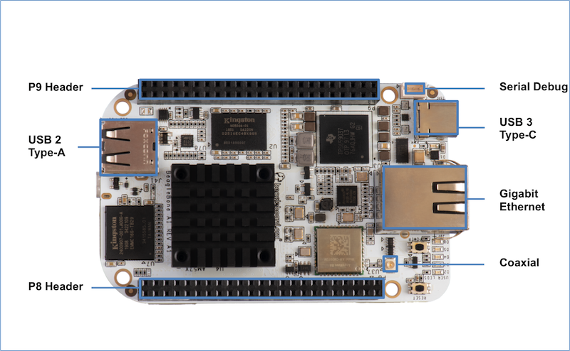

The expansion interface on the board is comprised of two 46 pin connectors, the P8 and P9 Headers. All signals on the expansion headers are 3.3V unless otherwise indicated.
NOTE: Do not connect 5V logic level signals to these pins or the board will be damaged.
NOTE: DO NOT APPLY VOLTAGE TO ANY I/O PIN WHEN POWER IS NOT SUPPLIED TO THE BOARD. IT WILL DAMAGE THE PROCESSOR AND VOID THE WARRANTY.
NO PINS ARE TO BE DRIVEN UNTIL AFTER THE SYS_RESET LINE GOES HIGH.
Figure ? shows the location of the expansion connectors.

The location and spacing of the expansion headers are the same as on BeagleBone Black.
The following tables show the pinout of the P8 expansion header. The SW is responsible for setting the default function of each pin. Refer to the processor documentation for more information on these pins and detailed descriptions of all of the pins listed. In some cases there may not be enough signals to complete a group of signals that may be required to implement a total interface.
The column heading is the pin number on the expansion header.
The GPIO row is the expected gpio identifier number in the Linux kernel.
The BALL row is the pin number on the processor.
The REG row is the offset of the control register for the processor pin.
The MODE # rows are the mode setting for each pin. Setting each mode to align with the mode column will give that function on that pin.
If included, the 2nd BALL row is the pin number on the processor for a second processor pin connected to the same pin on the expansion header. Similarly, all row headings starting with 2nd refer to data for this second processor pin.
NOTES:
DO NOT APPLY VOLTAGE TO ANY I/O PIN WHEN POWER IS NOT SUPPLIED TO THE BOARD. IT WILL DAMAGE THE PROCESSOR AND VOID THE WARRANTY.
NO PINS ARE TO BE DRIVEN UNTIL AFTER THE SYS_RESET LINE GOES HIGH.
| P8.03 | P8.04 | P8.05 | |
|---|---|---|---|
GPIO |
24 |
25 |
193 |
BALL |
AB8 |
AB5 |
AC9 |
REG |
0x179C |
0x17A0 |
0x178C |
MODE 0 |
mmc3_dat6 |
mmc3_dat7 |
mmc3_dat2 |
1 |
spi4_d0 |
spi4_cs0 |
spi3_cs0 |
2 |
uart10_ctsn |
uart10_rtsn |
uart5_ctsn |
3 |
|||
4 |
vin2b_de1 |
vin2b_clk1 |
vin2b_d3 |
5 |
|||
6 |
|||
7 |
|||
8 |
|||
9 |
vin5a_hsync0 |
vin5a_vsync0 |
vin5a_d3 |
10 |
ehrpwm3_tripzone_input |
eCAP3_in_PWM3_out |
eQEP3_index |
11 |
pr2_mii1_rxd1 |
pr2_mii1_rxd0 |
pr2_mii_mr1_clk |
12 |
pr2_pru0_gpi10 |
pr2_pru0_gpi11 |
pr2_pru0_gpi6 |
13 |
pr2_pru0_gpo10 |
pr2_pru0_gpo11 |
pr2_pru0_gpo6 |
14 |
gpio1_24 |
gpio1_25 |
gpio7_1 |
15 |
Driver off |
Driver off |
Driver off |
| P8.06 | P8.07 | P8.08 | P8.09 | |
|---|---|---|---|---|
GPIO |
194 |
165 |
166 |
178 |
BALL |
AC3 |
G14 |
F14 |
E17 |
REG |
0x1790 |
0x16EC |
0x16F0 |
0x1698 |
MODE 0 |
mmc3_dat3 |
mcasp1_axr14 |
mcasp1_axr15 |
xref_clk1 |
1 |
spi3_cs1 |
mcasp7_aclkx |
mcasp7_fsx |
mcasp2_axr9 |
2 |
uart5_rtsn |
mcasp7_aclkr |
mcasp7_fsr |
mcasp1_axr5 |
3 |
mcasp2_ahclkx |
|||
4 |
vin2b_d2 |
mcasp6_ahclkx |
||
5 |
||||
6 |
||||
7 |
vin6a_d9 |
vin6a_d8 |
vin6a_clk0 |
|
8 |
||||
9 |
vin5a_d2 |
|||
10 |
eQEP3_strobe |
timer11 |
timer12 |
timer14 |
11 |
pr2_mii1_rxdv |
pr2_mii0_rxdv |
pr2_mii0_rxd3 |
pr2_mii1_crs |
12 |
pr2_pru0_gpi7 |
pr2_pru1_gpi16 |
pr2_pru0_gpi20 |
pr2_pru1_gpi6 |
13 |
pr2_pru0_gpo7 |
pr2_pru1_gpo16 |
pr2_pru0_gpo20 |
pr2_pru1_gpo6 |
14 |
gpio7_2 |
gpio6_5 |
gpio6_6 |
gpio6_18 |
15 |
Driver off |
Driver off |
Driver off |
Driver off |
| P8.10 | P8.11 | P8.12 | P8.13 | |
|---|---|---|---|---|
GPIO |
164 |
75 |
74 |
107 |
BALL |
A13 |
AH4 |
AG6 |
D3 |
REG |
0x16E8 |
0x1510 |
0x150C |
0x1590 |
MODE 0 |
mcasp1_axr13 |
vin1a_d7 |
vin1a_d6 |
vin2a_d10 |
1 |
mcasp7_axr1 |
|||
2 |
||||
3 |
vout3_d0 |
vout3_d1 |
mdio_mclk |
|
4 |
vout3_d16 |
vout3_d17 |
vout2_d13 |
|
5 |
||||
6 |
||||
7 |
vin6a_d10 |
|||
8 |
||||
9 |
kbd_col7 |
|||
10 |
timer10 |
eQEP2B_in |
eQEP2A_in |
ehrpwm2B |
11 |
pr2_mii_mr0_clk |
pr1_mdio_mdclk |
||
12 |
pr2_pru1_gpi15 |
pr1_pru0_gpi4 |
pr1_pru0_gpi3 |
pr1_pru1_gpi7 |
13 |
pr2_pru1_gpo15 |
pr1_pru0_gpo4 |
pr1_pru0_gpo3 |
pr1_pru1_gpo7 |
14 |
gpio6_4 |
gpio3_11 |
gpio3_10 |
gpio4_11 |
15 |
Driver off |
Driver off |
Driver off |
Driver off |
| P8.14 | P8.15 | P8.16 | |
|---|---|---|---|
GPIO |
109 |
99 |
125 |
BALL |
D5 |
D1 |
B4 |
REG |
0x1598 |
0x1570 |
0x15BC |
MODE 0 |
vin2a_d12 |
vin2a_d2 |
vin2a_d21 |
1 |
|||
2 |
vin2b_d2 |
||
3 |
rgmii1_txc |
rgmii1_rxd2 |
|
4 |
vout2_d11 |
vout2_d21 |
vout2_d2 |
5 |
emu12 |
vin3a_fld0 |
|
6 |
vin3a_d13 |
||
7 |
|||
8 |
mii1_rxclk |
uart10_rxd |
mii1_col |
9 |
kbd_col8 |
kbd_row6 |
|
10 |
eCAP2_in_PWM2_out |
eCAP1_in_PWM1_out |
|
11 |
pr1_mii1_txd1 |
pr1_ecap0_ecap_capin_apwm_o |
pr1_mii1_rxlink |
12 |
pr1_pru1_gpi9 |
pr1_edio_data_in7 |
pr1_pru1_gpi18 |
13 |
pr1_pru1_gpo9 |
pr1_edio_data_out7 |
pr1_pru1_gpo18 |
14 |
gpio4_13 |
gpio4_3 |
gpio4_29 |
15 |
Driver off |
Driver off |
Driver off |
2nd BALL |
A3 |
||
2nd REG |
0x15B4 |
||
2nd MODE 0 |
vin2a_d19 |
||
2nd 1 |
|||
2nd 2 |
vin2b_d4 |
||
2nd 3 |
rgmii1_rxctl |
||
2nd 4 |
vout2_d4 |
||
2nd 5 |
|||
2nd 6 |
vin3a_d11 |
||
2nd 7 |
|||
2nd 8 |
mii1_txer |
||
2nd 9 |
|||
2nd 10 |
ehrpwm3_tripzone_input |
||
2nd 11 |
pr1_mii1_rxd0 |
||
2nd 12 |
pr1_pru1_gpi16 |
||
2nd 13 |
pr1_pru1_gpo16 |
||
2nd 14 |
gpio4_27 |
||
2nd 15 |
Driver off |
| P8.17 | P8.18 | P8.19 | |
|---|---|---|---|
GPIO |
242 |
105 |
106 |
BALL |
A7 |
F5 |
E6 |
REG |
0x1624 |
0x1588 |
0x158C |
MODE 0 |
vout1_d18 |
vin2a_d8 |
vin2a_d9 |
1 |
|||
2 |
emu4 |
||
3 |
vin4a_d2 |
||
4 |
vin3a_d2 |
vout2_d15 |
vout2_d14 |
5 |
obs11 |
emu18 |
emu19 |
6 |
obs27 |
||
7 |
|||
8 |
mii1_rxd3 |
mii1_rxd0 |
|
9 |
kbd_col5 |
kbd_col6 |
|
10 |
pr2_edio_data_in2 |
eQEP2_strobe |
ehrpwm2A |
11 |
pr2_edio_data_out2 |
pr1_mii1_txd3 |
pr1_mii1_txd2 |
12 |
pr2_pru0_gpi15 |
pr1_pru1_gpi5 |
pr1_pru1_gpi6 |
13 |
pr2_pru0_gpo15 |
pr1_pru1_gpo5 |
pr1_pru1_gpo6 |
14 |
gpio8_18 |
gpio4_9 |
gpio4_10 |
15 |
Driver off |
Driver off |
Driver off |
| P8.20 | P8.21 | P8.22 | |
|---|---|---|---|
GPIO |
190 |
189 |
23 |
BALL |
AC4 |
AD4 |
AD6 |
REG |
0x1780 |
0x177C |
0x1798 |
MODE 0 |
mmc3_cmd |
mmc3_clk |
mmc3_dat5 |
1 |
spi3_sclk |
spi4_d1 |
|
2 |
uart10_txd |
||
3 |
|||
4 |
vin2b_d6 |
vin2b_d7 |
vin2b_d0 |
5 |
|||
6 |
|||
7 |
|||
8 |
|||
9 |
vin5a_d6 |
vin5a_d7 |
vin5a_d0 |
10 |
eCAP2_in_PWM2_out |
ehrpwm2_tripzone_input |
ehrpwm3B |
11 |
pr2_mii1_txd2 |
pr2_mii1_txd3 |
pr2_mii1_rxd2 |
12 |
pr2_pru0_gpi3 |
pr2_pru0_gpi2 |
pr2_pru0_gpi9 |
13 |
pr2_pru0_gpo3 |
pr2_pru0_gpo2 |
pr2_pru0_gpo9 |
14 |
gpio6_30 |
gpio6_29 |
gpio1_23 |
15 |
Driver off |
Driver off |
Driver off |
| P8.23 | P8.24 | P8.25 | P8.26 | |
|---|---|---|---|---|
GPIO |
22 |
192 |
191 |
124 |
BALL |
AC8 |
AC6 |
AC7 |
B3 |
REG |
0x1794 |
0x1788 |
0x1784 |
0x15B8 |
MODE 0 |
mmc3_dat4 |
mmc3_dat1 |
mmc3_dat0 |
vin2a_d20 |
1 |
spi4_sclk |
spi3_d0 |
spi3_d1 |
|
2 |
uart10_rxd |
uart5_txd |
uart5_rxd |
vin2b_d3 |
3 |
rgmii1_rxd3 |
|||
4 |
vin2b_d1 |
vin2b_d4 |
vin2b_d5 |
vout2_d3 |
5 |
vin3a_de0 |
|||
6 |
vin3a_d12 |
|||
7 |
||||
8 |
mii1_rxer |
|||
9 |
vin5a_d1 |
vin5a_d4 |
vin5a_d5 |
|
10 |
ehrpwm3A |
eQEP3B_in |
eQEP3A_in |
eCAP3_in_PWM3_out |
11 |
pr2_mii1_rxd3 |
pr2_mii1_txd0 |
pr2_mii1_txd1 |
pr1_mii1_rxer |
12 |
pr2_pru0_gpi8 |
pr2_pru0_gpi5 |
pr2_pru0_gpi4 |
pr1_pru1_gpi17 |
13 |
pr2_pru0_gpo8 |
pr2_pru0_gpo5 |
pr2_pru0_gpo4 |
pr1_pru1_gpo17 |
14 |
gpio1_22 |
gpio7_0 |
gpio6_31 |
gpio4_28 |
15 |
Driver off |
Driver off |
Driver off |
Driver off |
| P8.27 | P8.28 | P8.29 | |
|---|---|---|---|
GPIO |
119 |
115 |
118 |
BALL |
E11 |
D11 |
C11 |
REG |
0x15D8 |
0x15C8 |
0x15D4 |
MODE 0 |
vout1_vsync |
vout1_clk |
vout1_hsync |
1 |
|||
2 |
|||
3 |
vin4a_vsync0 |
vin4a_fld0 |
vin4a_hsync0 |
4 |
vin3a_vsync0 |
vin3a_fld0 |
vin3a_hsync0 |
5 |
|||
6 |
|||
7 |
|||
8 |
spi3_sclk |
spi3_cs0 |
spi3_d0 |
9 |
|||
10 |
|||
11 |
|||
12 |
pr2_pru1_gpi17 |
||
13 |
pr2_pru1_gpo17 |
||
14 |
gpio4_23 |
gpio4_19 |
gpio4_22 |
15 |
Driver off |
Driver off |
Driver off |
2nd BALL |
A8 |
C9 |
A9 |
2nd REG |
0x1628 |
0x162C |
0x1630 |
2nd MODE 0 |
vout1_d19 |
vout1_d20 |
vout1_d21 |
2nd 1 |
|||
2nd 2 |
emu15 |
emu16 |
emu17 |
2nd 3 |
vin4a_d3 |
vin4a_d4 |
vin4a_d5 |
2nd 4 |
vin3a_d3 |
vin3a_d4 |
vin3a_d5 |
2nd 5 |
obs12 |
obs13 |
obs14 |
2nd 6 |
obs28 |
obs29 |
obs30 |
2nd 7 |
|||
2nd 8 |
|||
2nd 9 |
|||
2nd 10 |
pr2_edio_data_in3 |
pr2_edio_data_in4 |
pr2_edio_data_in5 |
2nd 11 |
pr2_edio_data_out3 |
pr2_edio_data_out4 |
pr2_edio_data_out5 |
2nd 12 |
pr2_pru0_gpi16 |
pr2_pru0_gpi17 |
pr2_pru0_gpi18 |
2nd 13 |
pr2_pru0_gpo16 |
pr2_pru0_gpo17 |
pr2_pru0_gpo18 |
2nd 14 |
gpio8_19 |
gpio8_20 |
gpio8_21 |
2nd 15 |
Driver off |
Driver off |
Driver off |
| P8.30 | P8.31 | P8.32 | |
|---|---|---|---|
GPIO |
116 |
238 |
239 |
BALL |
B10 |
C8 |
C7 |
REG |
0x15CC |
0x1614 |
0x1618 |
MODE 0 |
vout1_de |
vout1_d14 |
vout1_d15 |
1 |
|||
2 |
emu13 |
emu14 |
|
3 |
vin4a_de0 |
vin4a_d14 |
vin4a_d15 |
4 |
vin3a_de0 |
vin3a_d14 |
vin3a_d15 |
5 |
obs9 |
obs10 |
|
6 |
obs25 |
obs26 |
|
7 |
|||
8 |
spi3_d1 |
||
9 |
|||
10 |
pr2_uart0_txd |
pr2_ecap0_ecap_capin_apwm_o |
|
11 |
|||
12 |
pr2_pru0_gpi11 |
pr2_pru0_gpi12 |
|
13 |
pr2_pru0_gpo11 |
pr2_pru0_gpo12 |
|
14 |
gpio4_20 |
gpio8_14 |
gpio8_15 |
15 |
Driver off |
Driver off |
Driver off |
2nd BALL |
B9 |
G16 |
D17 |
2nd REG |
0x1634 |
0x173C |
0x1740 |
2nd MODE 0 |
vout1_d22 |
mcasp4_axr0 |
mcasp4_axr1 |
2nd 1 |
|||
2nd 2 |
emu18 |
spi3_d0 |
spi3_cs0 |
2nd 3 |
vin4a_d6 |
uart8_ctsn |
uart8_rtsn |
2nd 4 |
vin3a_d6 |
uart4_rxd |
uart4_txd |
2nd 5 |
obs15 |
||
2nd 6 |
obs31 |
vout2_d18 |
vout2_d19 |
2nd 7 |
|||
2nd 8 |
vin4a_d18 |
vin4a_d19 |
|
2nd 9 |
vin5a_d13 |
vin5a_d12 |
|
2nd 10 |
pr2_edio_data_in6 |
||
2nd 11 |
pr2_edio_data_out6 |
||
2nd 12 |
pr2_pru0_gpi19 |
pr2_pru1_gpi0 |
|
2nd 13 |
pr2_pru0_gpo19 |
pr2_pru1_gpo0 |
|
2nd 14 |
gpio8_22 |
||
2nd 15 |
Driver off |
Driver off |
Driver off |
| P8.33 | P8.34 | P8.35 | |
|---|---|---|---|
GPIO |
237 |
235 |
236 |
BALL |
C6 |
D8 |
A5 |
REG |
0x1610 |
0x1608 |
0x160C |
MODE 0 |
vout1_d13 |
vout1_d11 |
vout1_d12 |
1 |
|||
2 |
emu12 |
emu10 |
emu11 |
3 |
vin4a_d13 |
vin4a_d11 |
vin4a_d12 |
4 |
vin3a_d13 |
vin3a_d11 |
vin3a_d12 |
5 |
obs8 |
obs6 |
obs7 |
6 |
obs24 |
obs22 |
obs23 |
7 |
obs_dmarq2 |
||
8 |
|||
9 |
|||
10 |
pr2_uart0_rxd |
pr2_uart0_cts_n |
pr2_uart0_rts_n |
11 |
|||
12 |
pr2_pru0_gpi10 |
pr2_pru0_gpi8 |
pr2_pru0_gpi9 |
13 |
pr2_pru0_gpo10 |
pr2_pru0_gpo8 |
pr2_pru0_gpo9 |
14 |
gpio8_13 |
gpio8_11 |
gpio8_12 |
15 |
Driver off |
Driver off |
Driver off |
2nd BALL |
AF9 |
G6 |
AD9 |
2nd REG |
0x14E8 |
0x1564 |
0x14E4 |
2nd MODE 0 |
vin1a_fld0 |
vin2a_vsync0 |
vin1a_de0 |
2nd 1 |
vin1b_vsync1 |
vin1b_hsync1 |
|
2nd 2 |
|||
2nd 3 |
vin2b_vsync1 |
vout3_d17 |
|
2nd 4 |
vout3_clk |
vout2_vsync |
vout3_de |
2nd 5 |
uart7_txd |
emu9 |
uart7_rxd |
2nd 6 |
|||
2nd 7 |
timer15 |
uart9_txd |
timer16 |
2nd 8 |
spi3_d1 |
spi4_d1 |
spi3_sclk |
2nd 9 |
kbd_row1 |
kbd_row3 |
kbd_row0 |
2nd 10 |
eQEP1B_in |
ehrpwm1A |
eQEP1A_in |
2nd 11 |
pr1_uart0_rts_n |
||
2nd 12 |
pr1_edio_data_in4 |
||
2nd 13 |
pr1_edio_data_out4 |
||
2nd 14 |
gpio3_1 |
gpio4_0 |
gpio3_0 |
2nd 15 |
Driver off |
Driver off |
Driver off |
| P8.36 | P8.37 | P8.38 | |
|---|---|---|---|
GPIO |
234 |
232 |
233 |
BALL |
D7 |
E8 |
D9 |
REG |
0x1604 |
0x15FC |
0x1600 |
MODE 0 |
vout1_d10 |
vout1_d8 |
vout1_d9 |
1 |
|||
2 |
emu3 |
uart6_rxd |
uart6_txd |
3 |
vin4a_d10 |
vin4a_d8 |
vin4a_d9 |
4 |
vin3a_d10 |
vin3a_d8 |
vin3a_d9 |
5 |
obs5 |
||
6 |
obs21 |
||
7 |
obs_irq2 |
||
8 |
|||
9 |
|||
10 |
pr2_edio_sof |
pr2_edc_sync1_out |
pr2_edio_latch_in |
11 |
|||
12 |
pr2_pru0_gpi7 |
pr2_pru0_gpi5 |
pr2_pru0_gpi6 |
13 |
pr2_pru0_gpo7 |
pr2_pru0_gpo5 |
pr2_pru0_gpo6 |
14 |
gpio8_10 |
gpio8_8 |
gpio8_9 |
15 |
Driver off |
Driver off |
Driver off |
2nd BALL |
F2 |
A21 |
C18 |
2nd REG |
0x1568 |
0x1738 |
0x1734 |
2nd MODE 0 |
vin2a_d0 |
mcasp4_fsx |
mcasp4_aclkx |
2nd 1 |
mcasp4_fsr |
mcasp4_aclkr |
|
2nd 2 |
spi3_d1 |
spi3_sclk |
|
2nd 3 |
uart8_txd |
uart8_rxd |
|
2nd 4 |
vout2_d23 |
i2c4_scl |
i2c4_sda |
2nd 5 |
emu10 |
||
2nd 6 |
vout2_d17 |
vout2_d16 |
|
2nd 7 |
uart9_ctsn |
||
2nd 8 |
spi4_d0 |
vin4a_d17 |
vin4a_d16 |
2nd 9 |
kbd_row4 |
vin5a_d14 |
vin5a_d15 |
2nd 10 |
ehrpwm1B |
||
2nd 11 |
pr1_uart0_rxd |
||
2nd 12 |
pr1_edio_data_in5 |
||
2nd 13 |
pr1_edio_data_out5 |
||
2nd 14 |
gpio4_1 |
||
2nd 15 |
Driver off |
Driver off |
Driver off |
| P8.39 | P8.40 | P8.41 | |
|---|---|---|---|
GPIO |
230 |
231 |
228 |
BALL |
F8 |
E7 |
E9 |
REG |
0x15F4 |
0x15F8 |
0x15EC |
MODE 0 |
vout1_d6 |
vout1_d7 |
vout1_d4 |
1 |
|||
2 |
emu8 |
emu9 |
emu6 |
3 |
vin4a_d22 |
vin4a_d23 |
vin4a_d20 |
4 |
vin3a_d22 |
vin3a_d23 |
vin3a_d20 |
5 |
obs4 |
obs2 |
|
6 |
obs20 |
obs18 |
|
7 |
|||
8 |
|||
9 |
|||
10 |
pr2_edc_latch1_in |
pr2_edc_sync0_out |
pr1_ecap0_ecap_capin_apwm_o |
11 |
|||
12 |
pr2_pru0_gpi3 |
pr2_pru0_gpi4 |
pr2_pru0_gpi1 |
13 |
pr2_pru0_gpo3 |
pr2_pru0_gpo4 |
pr2_pru0_gpo1 |
14 |
gpio8_6 |
gpio8_7 |
gpio8_4 |
15 |
Driver off |
Driver off |
Driver off |
| P8.42 | P8.43 | P8.44 | |
|---|---|---|---|
GPIO |
229 |
226 |
227 |
BALL |
F9 |
F10 |
G11 |
REG |
0x15F0 |
0x15E4 |
0x15E8 |
MODE 0 |
vout1_d5 |
vout1_d2 |
vout1_d3 |
1 |
|||
2 |
emu7 |
emu2 |
emu5 |
3 |
vin4a_d21 |
vin4a_d18 |
vin4a_d19 |
4 |
vin3a_d21 |
vin3a_d18 |
vin3a_d19 |
5 |
obs3 |
obs0 |
obs1 |
6 |
obs19 |
obs16 |
obs17 |
7 |
obs_irq1 |
obs_dmarq1 |
|
8 |
|||
9 |
|||
10 |
pr2_edc_latch0_in |
pr1_uart0_rxd |
pr1_uart0_txd |
11 |
|||
12 |
pr2_pru0_gpi2 |
pr2_pru1_gpi20 |
pr2_pru0_gpi0 |
13 |
pr2_pru0_gpo2 |
pr2_pru1_gpo20 |
pr2_pru0_gpo0 |
14 |
gpio8_5 |
gpio8_2 |
gpio8_3 |
15 |
Driver off |
Driver off |
Driver off |
| P8.45 | P8.46 | |
|---|---|---|
GPIO |
224 |
225 |
BALL |
F11 |
G10 |
REG |
0x15DC |
0x15E0 |
MODE 0 |
vout1_d0 |
vout1_d1 |
1 |
||
2 |
uart5_rxd |
uart5_txd |
3 |
vin4a_d16 |
vin4a_d17 |
4 |
vin3a_d16 |
vin3a_d17 |
5 |
||
6 |
||
7 |
||
8 |
spi3_cs2 |
|
9 |
||
10 |
pr1_uart0_cts_n |
pr1_uart0_rts_n |
11 |
||
12 |
pr2_pru1_gpi18 |
pr2_pru1_gpi19 |
13 |
pr2_pru1_gpo18 |
pr2_pru1_gpo19 |
14 |
gpio8_0 |
gpio8_1 |
15 |
Driver off |
Driver off |
2nd BALL |
B7 |
A10 |
2nd REG |
0x161C |
0x1638 |
2nd MODE 0 |
vout1_d16 |
vout1_d23 |
2nd 1 |
||
2nd 2 |
uart7_rxd |
emu19 |
2nd 3 |
vin4a_d0 |
vin4a_d7 |
2nd 4 |
vin3a_d0 |
vin3a_d7 |
2nd 5 |
||
2nd 6 |
||
2nd 7 |
||
2nd 8 |
spi3_cs3 |
|
2nd 9 |
||
2nd 10 |
pr2_edio_data_in0 |
pr2_edio_data_in7 |
2nd 11 |
pr2_edio_data_out0 |
pr2_edio_data_out7 |
2nd 12 |
pr2_pru0_gpi13 |
pr2_pru0_gpi20 |
2nd 13 |
pr2_pru0_gpo13 |
pr2_pru0_gpo20 |
2nd 14 |
gpio8_16 |
gpio8_23 |
2nd 15 |
Driver off |
Driver off |
EOF
TODO: Notes regarding the resistors on muxed pins.
The following tables show the pinout of the P9 expansion header. The SW is responsible for setting the default function of each pin. Refer to the processor documentation for more information on these pins and detailed descriptions of all of the pins listed. In some cases there may not be enough signals to complete a group of signals that may be required to implement a total interface.
The column heading is the pin number on the expansion header.
The GPIO row is the expected gpio identifier number in the Linux kernel.
The BALL row is the pin number on the processor.
The REG row is the offset of the control register for the processor pin.
The MODE # rows are the mode setting for each pin. Setting each mode to align with the mode column will give that function on that pin.
If included, the 2nd BALL row is the pin number on the processor for a second processor pin connected to the same pin on the expansion header. Similarly, all row headings starting with 2nd refer to data for this second processor pin.
NOTES:
DO NOT APPLY VOLTAGE TO ANY I/O PIN WHEN POWER IS NOT SUPPLIED TO THE BOARD. IT WILL DAMAGE THE PROCESSOR AND VOID THE WARRANTY.
NO PINS ARE TO BE DRIVEN UNTIL AFTER THE SYS_RESET LINE GOES HIGH.
In the table are the following notations:
PWR_BUT is a 5V level as pulled up internally by the TPS6590379. It is activated by pulling the signal to GND.
TODO: (Actually, on BeagleBone AI, I believe PWR_BUT is pulled to 3.3V, but activation is still done by pulling the signal to GND. Also, a quick grounding of PWR_BUT will trigger a system event where shutdown can occur, but there is no hardware power-off function like on BeagleBone Black via this signal. It does, however, act as a hardware power-on.)
TODO: (On BeagleBone Black, SYS_RESET was a bi-directional signal, but it is only an output from BeagleBone AI to capes on BeagleBone AI.)
| P9.11 | P9.12 | P9.13 | |
|---|---|---|---|
GPIO |
241 |
128 |
172 |
BALL |
B19 |
B14 |
C17 |
REG |
0x172C |
0x16AC |
0x1730 |
MODE 0 |
mcasp3_axr0 |
mcasp1_aclkr |
mcasp3_axr1 |
1 |
mcasp7_axr2 |
||
2 |
mcasp2_axr14 |
mcasp2_axr15 |
|
3 |
uart7_ctsn |
uart7_rtsn |
|
4 |
uart5_rxd |
uart5_txd |
|
5 |
|||
6 |
vout2_d0 |
||
7 |
vin6a_d1 |
vin6a_d0 |
|
8 |
vin4a_d0 |
||
9 |
vin5a_fld0 |
||
10 |
i2c4_sda |
||
11 |
pr2_mii1_rxer |
pr2_mii1_rxlink |
|
12 |
pr2_pru0_gpi14 |
pr2_pru0_gpi15 |
|
13 |
pr2_pru0_gpo14 |
pr2_pru0_gpo15 |
|
14 |
gpio5_0 |
||
15 |
Driver off |
Driver off |
Driver off |
2nd BALL |
B8 |
AB10** |
|
2nd REG |
0x1620 |
0x1680 |
|
2nd MODE 0 |
vout1_d17 |
usb1_drvvbus |
|
2nd 1 |
|||
2nd 2 |
uart7_txd |
||
2nd 3 |
vin4a_d1 |
||
2nd 4 |
vin3a_d1 |
||
2nd 5 |
|||
2nd 6 |
|||
2nd 7 |
timer16 |
||
2nd 8 |
|||
2nd 9 |
|||
2nd 10 |
pr2_edio_data_in1 |
||
2nd 11 |
pr2_edio_data_out1 |
||
2nd 12 |
pr2_pru0_gpi14 |
||
2nd 13 |
pr2_pru0_gpo14 |
||
2nd 14 |
gpio8_17 |
gpio6_12 |
|
2nd 15 |
Driver off |
Driver off |
| P9.14 | P9.15 | P9.16 | |
|---|---|---|---|
GPIO |
121 |
76 |
122 |
BALL |
D6 |
AG4 |
C5 |
REG |
0x15AC |
0x1514 |
0x15B0 |
MODE 0 |
vin2a_d17 |
vin1a_d8 |
vin2a_d18 |
1 |
vin1b_d7 |
||
2 |
vin2b_d6 |
vin2b_d5 |
|
3 |
rgmii1_txd0 |
rgmii1_rxc |
|
4 |
vout2_d6 |
vout3_d15 |
vout2_d5 |
5 |
|||
6 |
vin3a_d9 |
vin3a_d10 |
|
7 |
|||
8 |
mii1_txd2 |
mii1_txd3 |
|
9 |
kbd_row2 |
||
10 |
ehrpwm3A |
eQEP2_index |
ehrpwm3B |
11 |
pr1_mii1_rxd2 |
pr1_mii1_rxd1 |
|
12 |
pr1_pru1_gpi14 |
pr1_pru0_gpi5 |
pr1_pru1_gpi15 |
13 |
pr1_pru1_gpo14 |
pr1_pru0_gpo5 |
pr1_pru1_gpo15 |
14 |
gpio4_25 |
gpio3_12 |
gpio4_26 |
15 |
Driver off |
Driver off |
Driver off |
| P9.17 | P9.18 | P9.19 | |
|---|---|---|---|
GPIO |
209 |
208 |
195 |
BALL |
B24 |
G17 |
R6 |
REG |
0x17CC |
0x17C8 |
0x1440 |
MODE 0 |
spi2_cs0 |
spi2_d0 |
gpmc_a0 |
1 |
uart3_rtsn |
uart3_ctsn |
|
2 |
uart5_txd |
uart5_rxd |
vin3a_d16 |
3 |
vout3_d16 |
||
4 |
vin4a_d0 |
||
5 |
|||
6 |
vin4b_d0 |
||
7 |
i2c4_scl |
||
8 |
uart5_rxd |
||
9 |
|||
10 |
|||
11 |
|||
12 |
|||
13 |
|||
14 |
gpio7_17 |
gpio7_16 |
gpio7_3 |
15 |
Driver off |
Driver off |
Driver off |
2nd BALL |
F12 |
G12 |
F4 |
2nd REG |
0x16B8 |
0x16B4 |
0x157C |
2nd MODE 0 |
mcasp1_axr1 |
mcasp1_axr0 |
vin2a_d5 |
2nd 1 |
|||
2nd 2 |
|||
2nd 3 |
uart6_txd |
uart6_rxd |
|
2nd 4 |
vout2_d18 |
||
2nd 5 |
emu15 |
||
2nd 6 |
|||
2nd 7 |
vin6a_hsync0 |
vin6a_vsync0 |
|
2nd 8 |
uart10_rtsn |
||
2nd 9 |
kbd_col2 |
||
2nd 10 |
i2c5_scl |
i2c5_sda |
eQEP2A_in |
2nd 11 |
pr2_mii_mt0_clk |
pr2_mii0_rxer |
pr1_edio_sof |
2nd 12 |
pr2_pru1_gpi9 |
pr2_pru1_gpi8 |
pr1_pru1_gpi2 |
2nd 13 |
pr2_pru1_gpo9 |
pr2_pru1_gpo8 |
pr1_pru1_gpo2 |
2nd 14 |
gpio5_3 |
gpio5_2 |
gpio4_6 |
2nd 15 |
Driver off |
Driver off |
Driver off |
| P9.20 | P9.21 | P9.22 | |
|---|---|---|---|
GPIO |
196 |
67 |
179 |
BALL |
T9 |
AF8 |
B26 |
REG |
0x1444 |
0x14F0 |
0x169C |
MODE 0 |
gpmc_a1 |
vin1a_vsync0 |
xref_clk2 |
1 |
vin1b_de1 |
mcasp2_axr10 |
|
2 |
vin3a_d17 |
mcasp1_axr6 |
|
3 |
vout3_d17 |
mcasp3_ahclkx |
|
4 |
vin4a_d1 |
vout3_vsync |
mcasp7_ahclkx |
5 |
uart7_rtsn |
||
6 |
vin4b_d1 |
vout2_clk |
|
7 |
i2c4_sda |
timer13 |
|
8 |
uart5_txd |
spi3_cs0 |
vin4a_clk0 |
9 |
|||
10 |
eQEP1_strobe |
timer15 |
|
11 |
|||
12 |
|||
13 |
|||
14 |
gpio7_4 |
gpio3_3 |
gpio6_19 |
15 |
Driver off |
Driver off |
Driver off |
2nd BALL |
D2 |
B22 |
A26 |
2nd REG |
0x1578 |
0x17C4 |
0x17C0 |
2nd MODE 0 |
vin2a_d4 |
spi2_d1 |
spi2_sclk |
2nd 1 |
uart3_txd |
uart3_rxd |
|
2nd 2 |
|||
2nd 3 |
|||
2nd 4 |
vout2_d19 |
||
2nd 5 |
emu14 |
||
2nd 6 |
|||
2nd 7 |
|||
2nd 8 |
uart10_ctsn |
||
2nd 9 |
kbd_col1 |
||
2nd 10 |
ehrpwm1_synco |
||
2nd 11 |
pr1_edc_sync0_out |
||
2nd 12 |
pr1_pru1_gpi1 |
||
2nd 13 |
pr1_pru1_gpo1 |
||
2nd 14 |
gpio4_5 |
gpio7_15 |
gpio7_14 |
2nd 15 |
Driver off |
Driver off |
Driver off |
| P9.23 | P9.24 | P9.25 | |
|---|---|---|---|
GPIO |
203 |
175 |
177 |
BALL |
A22 |
F20 |
D18 |
REG |
0x17B4 |
0x168C |
0x1694 |
MODE 0 |
spi1_cs1 |
gpio6_15 |
xref_clk0 |
1 |
mcasp1_axr9 |
mcasp2_axr8 |
|
2 |
sata1_led |
dcan2_rx |
mcasp1_axr4 |
3 |
spi2_cs1 |
uart10_txd |
mcasp1_ahclkx |
4 |
mcasp5_ahclkx |
||
5 |
|||
6 |
vout2_vsync |
||
7 |
vin6a_d0 |
||
8 |
vin4a_vsync0 |
hdq0 |
|
9 |
i2c3_scl |
clkout2 |
|
10 |
timer2 |
timer13 |
|
11 |
pr2_mii1_col |
||
12 |
pr2_pru1_gpi5 |
||
13 |
pr2_pru1_gpo5 |
||
14 |
gpio7_11 |
gpio6_15 |
gpio6_17 |
15 |
Driver off |
Driver off |
Driver off |
| P9.26 | P9.27 | P9.28 | P9.29 | |
|---|---|---|---|---|
GPIO |
174 |
111 |
113 |
139 |
BALL |
E21 |
C3 |
A12 |
A11 |
REG |
0x1688 |
0x15A0 |
0x16E0 |
0x16D8 |
MODE 0 |
gpio6_14 |
vin2a_d14 |
mcasp1_axr11 |
mcasp1_axr9 |
1 |
mcasp1_axr8 |
mcasp6_fsx |
mcasp6_axr1 |
|
2 |
dcan2_tx |
mcasp6_fsr |
||
3 |
uart10_rxd |
rgmii1_txd3 |
spi3_cs0 |
spi3_d1 |
4 |
vout2_d9 |
|||
5 |
||||
6 |
vout2_hsync |
|||
7 |
vin6a_d12 |
vin6a_d14 |
||
8 |
vin4a_hsync0 |
mii1_txclk |
||
9 |
i2c3_sda |
|||
10 |
timer1 |
eQEP3B_in |
timer8 |
timer6 |
11 |
pr1_mii_mr1_clk |
pr2_mii0_txd1 |
pr2_mii0_txd3 |
|
12 |
pr1_pru1_gpi11 |
pr2_pru1_gpi13 |
pr2_pru1_gpi11 |
|
13 |
pr1_pru1_gpo11 |
pr2_pru1_gpo13 |
pr2_pru1_gpo11 |
|
14 |
gpio6_14 |
gpio4_15 |
gpio4_17 |
gpio5_11 |
15 |
Driver off |
Driver off |
Driver off |
Driver off |
2nd BALL |
AE2 |
J14 |
D14 |
|
2nd REG |
0x1544 |
0x16B0 |
0x16A8 |
|
2nd MODE 0 |
vin1a_d20 |
mcasp1_fsr |
mcasp1_fsx |
|
2nd 1 |
vin1b_d3 |
mcasp7_axr3 |
||
2nd 2 |
||||
2nd 3 |
||||
2nd 4 |
vout3_d3 |
|||
2nd 5 |
||||
2nd 6 |
vin3a_d4 |
vout2_d1 |
||
2nd 7 |
vin6a_de0 |
|||
2nd 8 |
vin4a_d1 |
|||
2nd 9 |
kbd_col5 |
|||
2nd 10 |
pr1_edio_data_in4 |
i2c4_scl |
i2c3_scl |
|
2nd 11 |
pr1_edio_data_out4 |
pr2_mdio_data |
||
2nd 12 |
pr1_pru0_gpi17 |
|||
2nd 13 |
pr1_pru0_gpo17 |
|||
2nd 14 |
gpio3_24 |
gpio5_1 |
gpio7_30 |
|
2nd 15 |
Driver off |
Driver off |
Driver off |
| P9.30 | P9.31 | |
|---|---|---|
GPIO |
140 |
138 |
BALL |
B13 |
B12 |
REG |
0x16DC |
0x16D4 |
MODE 0 |
mcasp1_axr10 |
mcasp1_axr8 |
1 |
mcasp6_aclkx |
mcasp6_axr0 |
2 |
mcasp6_aclkr |
|
3 |
spi3_d0 |
spi3_sclk |
4 |
||
5 |
||
6 |
||
7 |
vin6a_d13 |
vin6a_d15 |
8 |
||
9 |
||
10 |
timer7 |
timer5 |
11 |
pr2_mii0_txd2 |
pr2_mii0_txen |
12 |
pr2_pru1_gpi12 |
pr2_pru1_gpi10 |
13 |
pr2_pru1_gpo12 |
pr2_pru1_gpo10 |
14 |
gpio5_12 |
gpio5_10 |
15 |
Driver off |
Driver off |
2nd BALL |
C14 |
|
2nd REG |
0x16A4 |
|
2nd MODE 0 |
mcasp1_aclkx |
|
2nd 1 |
||
2nd 2 |
||
2nd 3 |
||
2nd 4 |
||
2nd 5 |
||
2nd 6 |
||
2nd 7 |
vin6a_fld0 |
|
2nd 8 |
||
2nd 9 |
||
2nd 10 |
i2c3_sda |
|
2nd 11 |
pr2_mdio_mdclk |
|
2nd 12 |
pr2_pru1_gpi7 |
|
2nd 13 |
pr2_pru1_gpo7 |
|
2nd 14 |
gpio7_31 |
|
2nd 15 |
Driver off |
| P9.41 | P9.42 | |
|---|---|---|
GPIO |
180 |
114 |
BALL |
C23 |
E14 |
REG |
0x16A0 |
0x16E4 |
MODE 0 |
xref_clk3 |
mcasp1_axr12 |
1 |
mcasp2_axr11 |
mcasp7_axr0 |
2 |
mcasp1_axr7 |
|
3 |
mcasp4_ahclkx |
spi3_cs1 |
4 |
mcasp8_ahclkx |
|
5 |
||
6 |
vout2_de |
|
7 |
hdq0 |
vin6a_d11 |
8 |
vin4a_de0 |
|
9 |
clkout3 |
|
10 |
timer16 |
timer9 |
11 |
pr2_mii0_txd0 |
|
12 |
pr2_pru1_gpi14 |
|
13 |
pr2_pru1_gpo14 |
|
14 |
gpio6_20 |
gpio4_18 |
15 |
Driver off |
Driver off |
2nd BALL |
C1 |
C2 |
2nd REG |
0x1580 |
0x159C |
2nd MODE 0 |
vin2a_d6 |
vin2a_d13 |
2nd 1 |
||
2nd 2 |
||
2nd 3 |
rgmii1_txctl |
|
2nd 4 |
vout2_d17 |
vout2_d10 |
2nd 5 |
emu16 |
|
2nd 6 |
||
2nd 7 |
||
2nd 8 |
mii1_rxd1 |
mii1_rxdv |
2nd 9 |
kbd_col3 |
kbd_row8 |
2nd 10 |
eQEP2B_in |
eQEP3A_in |
2nd 11 |
pr1_mii_mt1_clk |
pr1_mii1_txd0 |
2nd 12 |
pr1_pru1_gpi3 |
pr1_pru1_gpi10 |
2nd 13 |
pr1_pru1_gpo3 |
pr1_pru1_gpo10 |
2nd 14 |
gpio4_7 |
gpio4_14 |
2nd 15 |
Driver off |
Driver off |
There is a Cape Headers Google Spreadsheet which has a lot of detail regarding various boards and cape add-on boards.
TODO
TODO
This section is about both UART pins on the header and PRU UART pins on the headers we will include a chart and later some code
| Function | Pin | ABC Ball | Pinctrl Register | Mode |
|---|---|---|---|---|
uart3_txd |
P9.21 |
B22 |
0x17C4 |
1 |
uart3_rxd |
P9.22 |
A26 |
0x17C0 |
1 |
uart5_txd |
P9.13 |
C17 |
0x1730 |
4 |
uart5_rxd |
P9.11 |
B19 |
0x172C |
4 |
uart5_ctsn |
P8.05 |
AC9 |
0x178C |
2 |
uart5_rtsn |
P8.06 |
AC3 |
0x1790 |
2 |
uart8_txd |
P8.37 |
A21 |
0x1738 |
3 |
uart8_rxd |
P8.38 |
C18 |
0x1734 |
3 |
uart8_ctsn |
P8.31 |
G16 |
0x173C |
3 |
uart8_rtsn |
P8.32 |
D17 |
0x1740 |
3 |
uart10_txd |
P9.24 |
F20 |
0x168C |
3 |
uart10_rxd |
P9.26 |
E21 |
0x1688 |
3 |
uart10_ctsn |
P8.03 |
AB8 |
0x179C |
2 |
uart10_rtsn |
P8.04 |
AB5 |
0x17A0 |
2 |
uart10_txd |
P9.24 |
F20 |
0x168C |
3 |
uart10_rxd |
P9.26 |
E21 |
0x1688 |
3 |
uart10_ctsn |
P9.20 |
D2 |
0x1578 |
8 |
uart10_rtsn |
P9.19 |
F4 |
0x157C |
8 |
| Function | Pin | ABC Ball | Pinctrl Register | Mode |
|---|---|---|---|---|
pr2_uart0_txd |
P8.31 |
C8 |
0x1614 |
10 |
pr2_uart0_rxd |
P8.33 |
C6 |
0x1610 |
10 |
pr2_uart0_cts_n |
P8.34 |
D8 |
0x1608 |
10 |
pr2_uart0_rts_n |
P8.35 |
A5 |
0x160C |
10 |
pr1_uart0_rxd |
P8.43 |
F10 |
0x15E4 |
10 |
pr1_uart0_txd |
P8.44 |
G11 |
0x15E8 |
10 |
pr1_uart0_cts_n |
P8.45 |
F11 |
0x15DC |
10 |
pr1_uart0_rts_n |
P8.46 |
G10 |
0x15E0 |
10 |
TODO
TODO: discuss header options for working with the expansion connectors per https://github.com/beagleboard/beaglebone-black/wiki/System-Reference-Manual#84-expansion-connectors
-
Board Dimensions: 8.9cm x 5.4cm x 1.5cm
-
Board Net Weight 48g
-
Packaging Dimensions: 13.8cm x 10cm x 4cm
-
Gross Weight (including packaging): 110g
-
3D STEP model: https://github.com/beagleboard/beaglebone-ai/tree/master/Mechanical
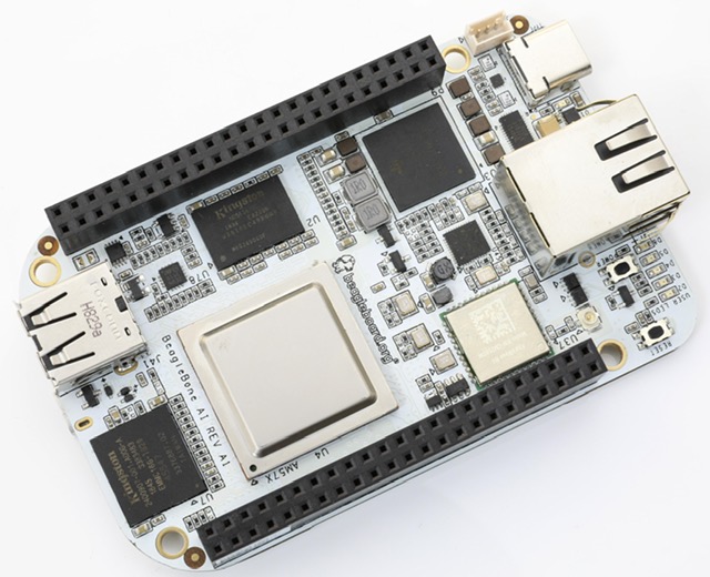
TODO: Reference https://beagleboard.org/support and https://beagleboard.org/resources
Related TI documentation: http://www.ti.com/tool/BEAGLE-3P-BBONE-AI
-
Country of origin: PRC
-
FCC: 2ATUT-BBONE-AI
-
CE: TBD
-
CNHTS: 8543909000
-
USHTS: 8473301180
-
MXHTS: 84733001
-
TARIC: 8473302000
-
ECCN: 5A992.C
-
CCATS: Z1613110/G180570
-
RoHS/REACH: TBD
-
Volatility: TBD
BeagleBone AI is annotated to comply with Part 15 of the FCC Rules. Operation is subject to the following two conditions: (1) This device may not cause harmful interference, and (2) this device must accept any interference received, including interference that may cause undesired operation. Changes or modifications not expressly approved by the party responsible for compliance could void the user’s authority to operate the equipment.
This Class A or B digital apparatus complies with Canadian ICES-003. Changes or modifications not expressly approved by the party responsible for compliance could void the user’s authority to operate the equipment. Cet appareil numérique de la classe A ou B est conforme à la norme NMB-003 du Canada. Les changements ou les modifications pas expressément approuvés par la partie responsible de la conformité ont pu vider l’autorité de l’utilisateur pour actionner l’équipement.
The design materials referred to in this document are *NOT SUPPORTED* and DO NOT constitute a reference design. Support of the open source developer community is provided through the the resources defined at https://beagleboard.org/support.
THERE IS NO WARRANTY FOR THE DESIGN MATERIALS, TO THE EXTENT PERMITTED BY APPLICABLE LAW. EXCEPT WHEN OTHERWISE STATED IN WRITING THE COPYRIGHT HOLDERS AND/OR OTHER PARTIES PROVIDE THE DESIGN MATERIALS “AS IS” WITHOUT WARRANTY OF ANY KIND, EITHER EXPRESSED OR IMPLIED, INCLUDING, BUT NOT LIMITED TO, THE IMPLIED WARRANTIES OF MERCHANTABILITY AND FITNESS FOR A PARTICULAR PURPOSE. THE ENTIRE RISK AS TO THE QUALITY AND PERFORMANCE OF THE DESIGN MATERIALS IS WITH YOU. SHOULD THE DESIGN MATERIALS PROVE DEFECTIVE, YOU ASSUME THE COST OF ALL NECESSARY SERVICING, REPAIR OR CORRECTION.
This board was designed as an evaluation and development tool. It was not designed with any other application in mind. As such, the design materials that are provided which include schematic, BOM, and PCB files, may or may not be suitable for any other purposes. If used, the design material becomes your responsibility as to whether or not it meets your specific needs or your specific applications and may require changes to meet your requirements.
BeagleBoard.org Foundation and logo-licensed manufacturers (together, henceforth identified as "Supplier") provide BeagleBone AI under the following conditions:
The user assumes all responsibility and liability for proper and safe handling of the goods. Further, the user indemnifies Supplier from all claims arising from the handling or use of the goods.
Should BeagleBone AI not meet the specifications indicated in the System Reference Manual, BeagleBone AI may be returned within 90 days from the date of delivery to the distributor of purchase for a full refund. THE FOREGOING LIMITED WARRANTY IS THE EXCLUSIVE WARRANTY MADE BY SELLER TO BUYER AND IS IN LIEU OF ALL OTHER WARRANTIES, EXPRESSED, IMPLIED, OR STATUTORY, INCLUDING ANY WARRANTY OF MERCHANTABILITY OR FITNESS FOR ANY PARTICULAR PURPOSE. EXCEPT TO THE EXTENT OF THE INDEMNITY SET FORTH ABOVE, NEITHER PARTY SHALL BE LIABLE TO THE OTHER FOR ANY INDIRECT, SPECIAL, INCIDENTAL, OR CONSEQUENTIAL DAMAGES.
Please read the System Reference Manual and, specifically, the Warnings and Restrictions notice in the Systems Reference Manual prior to handling the product. This notice contains important safety information about temperatures and voltages.
No license is granted under any patent right or other intellectual property right of Supplier covering or relating to any machine, process, or combination in which such Supplier products or services might be or are used. The Supplier currently deals with a variety of customers for products, and therefore our arrangement with the user is not exclusive. The Supplier assume no liability for applications assistance, customer product design, software performance, or infringement of patents or services described herein.
BeagleBone AI is not a complete product. It is intended solely for use for preliminary feasibility evaluation in laboratory/development environments by technically qualified electronics experts who are familiar with the dangers and application risks associated with handling electrical mechanical components, systems and subsystems. It should not be used as all or part of a finished end product.
You acknowledge, represent, and agree that:
-
You have unique knowledge concerning Federal, State and local regulatory requirements (including but not limited to Food and Drug Administration regulations, if applicable) which relate to your products and which relate to your use (and/or that of your employees, affiliates, contractors or designees) of BeagleBone AI for evaluation, testing and other purposes.
-
You have full and exclusive responsibility to assure the safety and compliance of your products with all such laws and other applicable regulatory requirements, and also to assure the safety of any activities to be conducted by you and/or your employees, affiliates, contractors or designees, using BeagleBone AI. Further, you are responsible to assure that any interfaces (electronic and/or mechanical) between BeagleBone AI and any human body are designed with suitable isolation and means to safely limit accessible leakage currents to minimize the risk of electrical shock hazard.
-
Since BeagleBone AI is not a completed product, it may not meet all applicable regulatory and safety compliance standards which may normally be associated with similar items. You assume full responsibility to determine and/or assure compliance with any such standards and related certifications as may be applicable. You will employ reasonable safeguards to ensure that your use of BeagleBone AI will not result in any property damage, injury or death, even if BeagleBone AI should fail to perform as described or expected.
It is important to operate BeagleBone AI within Supplier’s recommended specifications and environmental considerations per the user guidelines. Exceeding the specified BeagleBone AI ratings (including but not limited to input and output voltage, current, power, and environmental ranges) may cause property damage, personal injury or death. If there are questions concerning these ratings please contact the Supplier representative prior to connecting interface electronics including input power and intended loads. Any loads applied outside of the specified output range may result in unintended and/or inaccurate operation and/or possible permanent damage to BeagleBone AI and/or interface electronics. Please consult the System Reference Manual prior to connecting any load to BeagleBone AI output. If there is uncertainty as to the load specification, please contact the Supplier representative. During normal operation, some circuit components may have case temperatures greater than 60 C as long as the input and output are maintained at a normal ambient operating temperature. These components include but are not limited to linear regulators, switching transistors, pass transistors, and current sense resistors which can be identified using BeagleBone AI’s schematic located at the link in BeagleBone AI’s System Reference Manual. When placing measurement probes near these devices during normal operation, please be aware that these devices may be very warm to the touch. As with all electronic evaluation tools, only qualified personnel knowledgeable in electronic measurement and diagnostics normally found in development environments should use BeagleBone AI.
You agree to defend, indemnify and hold Supplier, its licensors and their representatives harmless from and against any and all claims, damages, losses, expenses, costs and liabilities (collectively, "Claims") arising out of or in connection with any use of BeagleBone AI that is not in accordance with the terms of the agreement. This obligation shall apply whether Claims arise under law of tort or contract or any other legal theory, and even if BeagleBone AI fails to perform as described or expected.
If you intend to evaluate the components for possible use in safety critical applications (such as life support) where a failure of the Supplier’s product would reasonably be expected to cause severe personal injury or death, such as devices which are classified as FDA Class III or similar classification, then you must specifically notify Supplier of such intent and enter into a separate Assurance and Indemnity Agreement.