-
Notifications
You must be signed in to change notification settings - Fork 0
Home
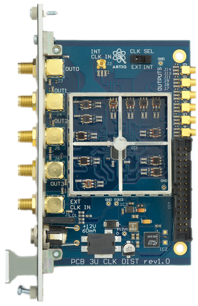
Low noise clock distribution module. The module can be used to distribute low jitter clock signal among EEMs.
Design files (schematics, PCB layouts, BOMs) can be found at Clocker/releases.
- 2 inputs (12 dBm < P < 15 dBm, #12 )
- 10 outputs including 4 SMAs
- frequency up to 1GHz
- low jitter <100fs RMS
- 3U EEM format
- 12V supply from EEM connector or front panel DC jack

As with other low-noise systems, it's important to avoid ground loops in the clock distribution network; ground loops can can introduce low-frequency (<1MHz) noise that seriously degrades the close-in phase noise of the transmitted clock. To avoid ground loops, this board adopts a "hybrid ground" strategy, whereby the source and receiver grounds are connected at the signal frequencies, but not at DC.
In an ideal world, for low frequencies the cable shield should be connected to electrical ground at the source end, but not at the receiver end. In practice this is not always possible, but it is nonetheless important to make sure that the cable is connected to ground at either (but not both) the source or receiver ground. By default, all input and output cable grounds are terminated to the clock buffer PCB/case/PSU ground via a high DC impedance (100k in parallel with 20nF). If the cable ground is connected to circuit ground at the other end, leave the cable ground floating at the buffer board. If the cable ground is floating at the other end, consider replacing the 10nF capacitors on the clock buffer board with 0R resistors to provide a good DC ground connection at the buffer board.