-
Notifications
You must be signed in to change notification settings - Fork 1
Hardware_details
| Description | Symbol | Value | Unit | |
|---|---|---|---|---|
| Min. | Max. | |||
| Input voltage power supply | Vcc | 2 | 3.6 | V |
| Average current consumption @3Vdc | Icc | - | - | - |
| Idle mode | - | TBC | uA | |
| CW @14dBm | - | 42 | mA | |
| Maximum Radio power conducted | Prf | 15 | dBm | |
| Operational temperature | T(°C) | -20 | 60 | °C |
| Digital Input Level High (Vdd 3V) | VIH | 2.1 | 3 | Vcc |
| Digital Input Level Low (Vdd 3V) | VIL | 0.0 | 0.9 | Vcc |
Warning
Please be aware that power supply impedance have to be as low as possible in order to ensure reliable transmission & modulation. If the internal serial resistance of the battery used to power your device is not < few Ohms, please consider voltage regulators to stabilize power supply during the radio burst.
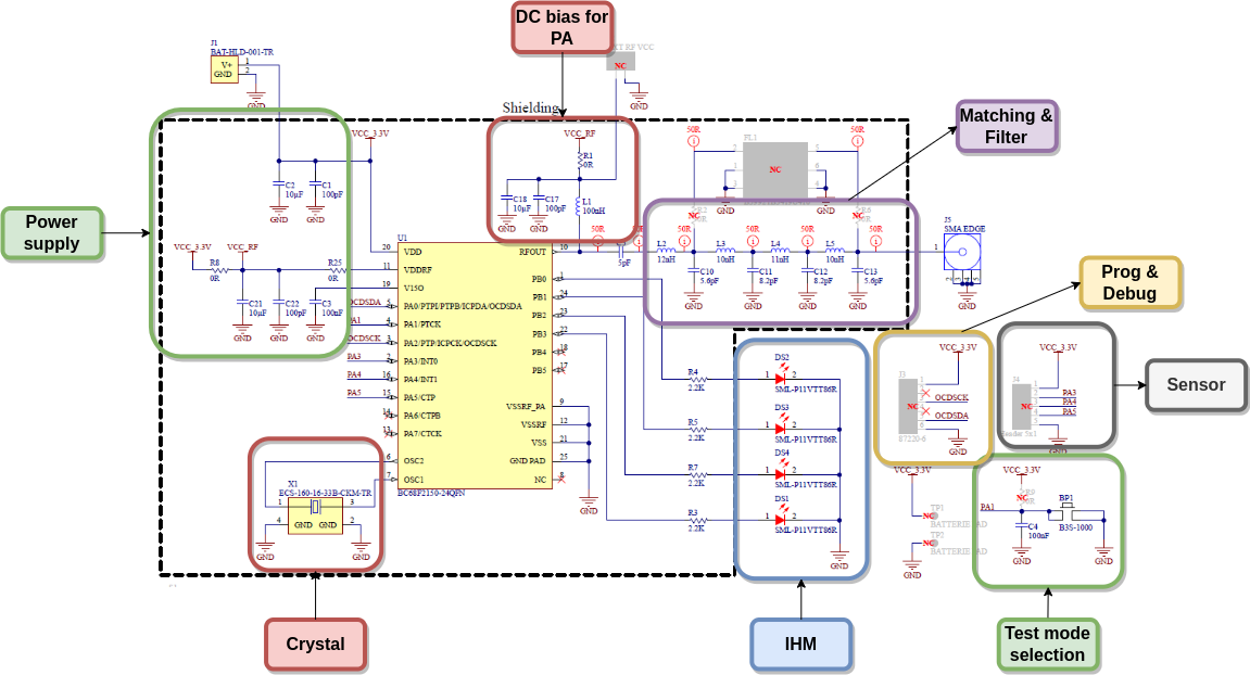
Recommandation from Holtek : Holtek suggested adding a resistor to RFOUT, it will help to adjust if the radiation leaks.

The following components need to be equipped : L2, L3, L4, L5, C10, C11, C12 and C13
Warning
The shielding is mandatory for RC2 configuration

The following components need to be equipped : R2 and R6 = 0ohm, FL1 SAW filter ref : B39921B3419U41, C10 = 1pF and L2 = 0ohm
Warning
L2, L3, L4, L5, C11, C12 and C13 are not equipped
Crystal selection is a critical part of the design for any Radio system. here is an example of crystal parameters chosen in this ref design.
Warning
The final design have to be compliant with Sigfox specification : see REF 4
| Description | Symbol | Value | Unit | |
|---|---|---|---|---|
| Min. | Max. | |||
| Frequency | F | 16 | 16 | MHz |
| Load Capacitor | Cl | 12 | 20 | pF |
| Frequency aging | +/-1 | ppm/year | ||
| Frequency tolerance @+25°C | Ftol | - | +/-10 | ppm |
| Frequency temperature tolerance | Ftemp | - | +/-10 | ppm |
| ESR | ESR | - | 40 | Ω |
The reference that was used in the ref design is : ECS-160-16-33B-CKM-TR but we have also validated ref. : ECS-160-CDX-2469 and FTR5244-A0/16.000MHz Rakon
The programming connector is directly compatible with the Holtek 8-bit MCU debug adapter e-link
You can buy the e-link here : were

| Signal Name | I/O | J3 Pin Number |
Descriptions |
|---|---|---|---|
| VCC | I | 1 | Power supply |
| NC | 2 | ||
| PA2-OCDSCK | I | 3 | Serial programming clock |
| NC | 4 | ||
| PA0-OCDSDA | I/O | 5 | Serial programming data |
| GND | I | 6 | Ground |
This connector has been placed in order to supply the Ref design by a Power supply, or battery.
| Signal Name | I/O | J 1 Pin Number |
Descriptions |
|---|---|---|---|
| VCC | I | 1 | Power supply (2 to 3.6V) |
| GND | I | 2 | GROUND |
This connector has been placed in order to allow some sensors connection. (no implementation in the firmware provided)
| Signal Name | I/O | J4 Pin Number |
Descriptions |
|---|---|---|---|
| VCC | I | 1 | Power supply |
| PA3 | I/O | 2 | I/O for sensor |
| PA4 | I/O | 3 | I/O for sensor |
| PA5 | I/O | 4 | I/O for sensor |
| GND | I | 5 | Ground |
- 1. Introduction
- 2. Sigfox
- 3. Firmware details
- 4. Hardware details
-
5. Sigfox RF & PROTOCOL Test Report
- 5.1. RFP RC1 100bps low power
- 5.2. RFP RC1 100bps high power
- 5.3. RFP RC2 600Bps "upcoming"
- 6. Radio test reports
